

Organic composition
a technology of organic composition and conductive line, applied in the field of organic composition, can solve the problems of increased current consumption, increased capacitance between neighbouring conductive lines, increased current consumption, etc., and achieve the effect of improving solubility and being more commercially attractiv
- Summary
- Abstract
- Description
- Claims
- Application Information
AI Technical Summary
Benefits of technology
Problems solved by technology
Method used
Image

Examples
##ventive example 1
INVENTIVE EXAMPLE 1
(Referred to Herein as “IE1”)
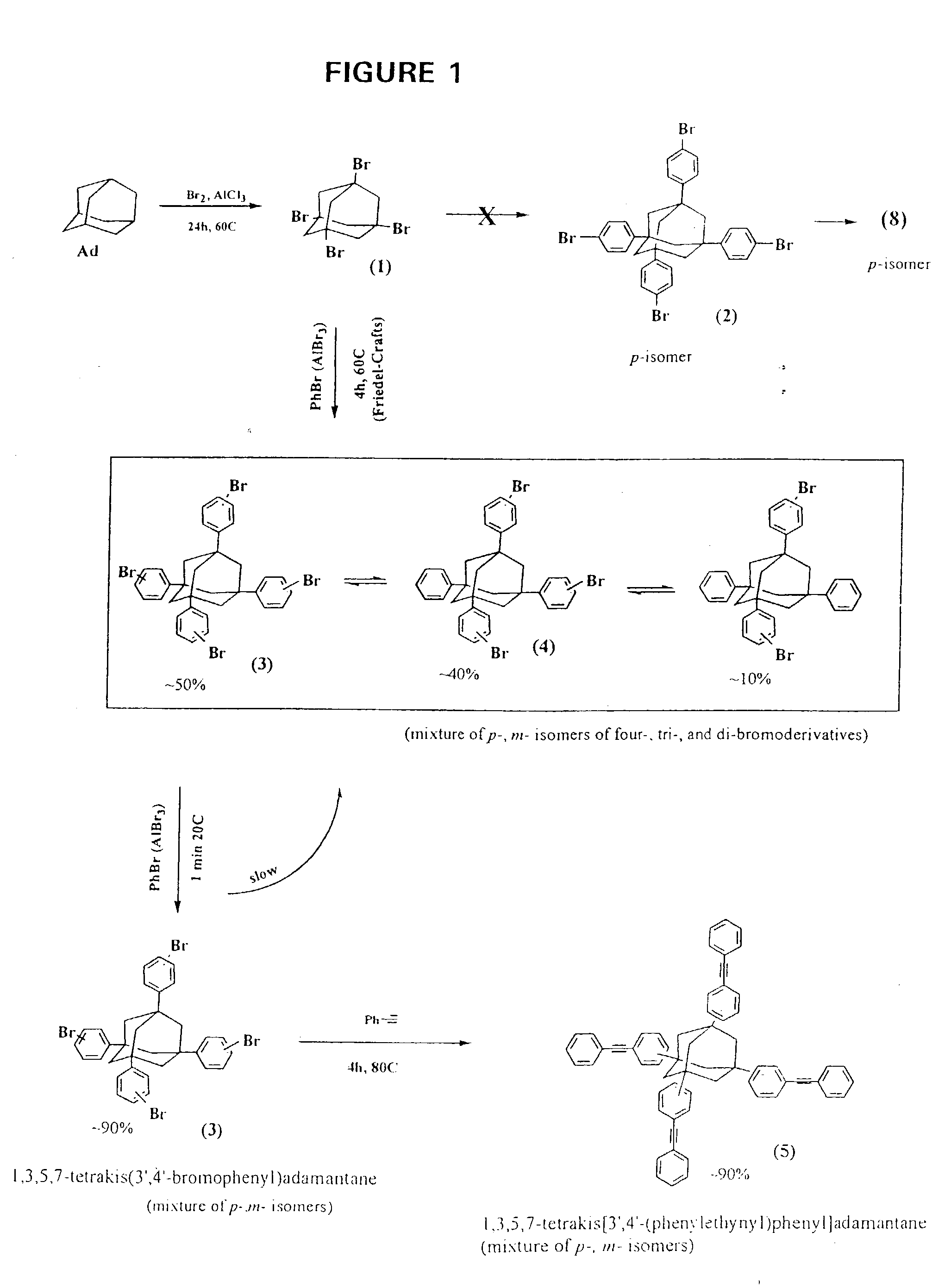
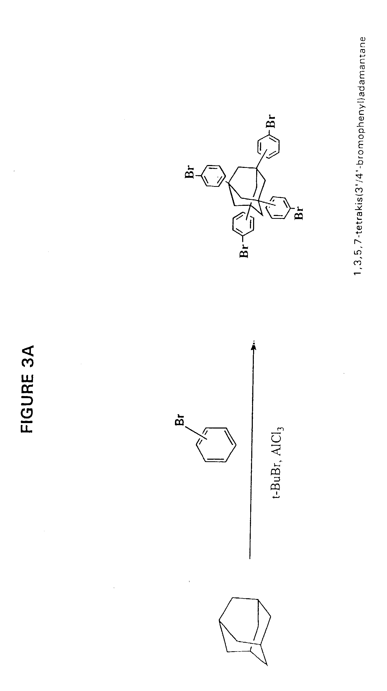
[0149] Step (a): Preparation of Mixture of [0150] 1,3,5,7-tetrakis(3′ / 4′-bromophenyl)adamantane (shown in FIG. 3A); [0151] 1,3 / 4-bis[1′,3′,5′-tris(3″ / 4″-bromophenyl)adamant-7′-yl]benzene (shown in FIG. 3C); and [0152] at least 1,3-bis{3′ / 4′-[1″,3″,5″-tris(3′″ / 4′″-bromophenyl)adamant-7″-yl]phenyl}-5,7-bis(3″″ / 4″″-bromophenyl)adamantane (shown in FIG. 3C) (collectively “IE1 Step (a) Product”)
[0153] A first reaction vessel was loaded with adamantane (200 grams), bromobenzene (1550 milliliters), and aluminum trichloride (50 grams). The reaction mixture was heated to 40° C. by a thermostatted water bath. Tert-butyl bromide (1206 grams) was added slowly over a period of 4-6 hours to the reaction mixture. The reaction mixture at 40° C. was stirred overnight.
[0154] A second reaction vessel was loaded with 1000 milliliters of aqueous hydrogen chloride (5% w / w). The contents of the first reaction vessel were gradually discharged into the seco...
##ventive example 2
INVENTIVE EXAMPLE 2
(Referred to Herein as “IE2”)
[0179] Step (a): Preparation of Mixture of [0180] 1,3,5,7-tetrakis(3′ / 4′-bromophenyl)adamantane (shown in FIG. 3A); [0181] 1,3 / 4-bis[′,3′,5′-tris(3″ / 4″-bromophenyl)adamant-7′-yl]benzene (shown in FIG. 3C); and at least [0182] 1,3-bis{3′ / 4′-[1″,3″,5″-tris(3′″ / 4′″-bromophenyl)adamant-7″-yl]phenyl}-5,7-bis(3″″ / 4″″-bromophenyl)adamantane(shown in FIG. 3C)(collectively “IE2 Step (a) Product”)
[0183] A first reaction vessel was loaded with 1,4-dibromobenzene (587.4 grams) and aluminum trichloride (27.7 grams). This reaction mixture was heated to 90° C. by a thermostatted water bath and maintained at this temperature for one hour without stirring and for an additional one hour with stirring. The reaction mixture was cooled down to 50° C. Adamantane (113.1 grams) was added to the cooled reaction mixture. Over a period of four hours, t-butyl-bromobenzene (796.3 grams) was added to the reaction mixture. The reaction mixture was stirred for an a...
##ventive example 3
INVENTIVE EXAMPLE 3
[0209] Impact of Solvent on ratio of 1,3,5,7-tetrakis[3′,4′-(phenylethynyl)phenyl]adamantane (shown in FIG. 3D) to 1,3 / 4-bis{1′,3′,5′-tris[3″ / 4″-phenylethynyl)phenyl]adamant-7′-yl} benzene (shown in FIG. 3F) and at least 1,3-bis{3′ / 4′-[1″,3″,5″-tris[3′″ / 4′″-(phenylethynyl)phenyl]adamant-7″-yl]phenyl}-5,7-bis[3″″ / 4″″-(phenylethynyl phenyl]adamantane (shown in FIG. 3F)
[0210] 5 850 milliliters of IE1 Step (a) Product was divided into four equal parts, and subjected to precipitation in petroleum ether, ligroine, heptane, and methanol. Each part was precipitated into 2520 ml of the solvent, vacuum filtered (Buchner funnel diam. 185 mm), washed on filter twice by 150 ml of the solvent, then dried in a vacuum oven for two hours at about 20° C., overnight at 40° C., and at 70-80° C. to constant weight.
[0211] Precipitation into hydrocarbons resulted in very dispersed light beige powders that dried without complications. Precipitation into methanol gave heavy, brownish gr...
PUM
| Property | Measurement | Unit |
|---|---|---|
| Thickness | aaaaa | aaaaa |
| Transition temperature | aaaaa | aaaaa |
| Fraction | aaaaa | aaaaa |
Abstract
Description
Claims
Application Information