Thin film optical detectors for retinal implantation and methods for making and using same

a technology of optical detectors and retinal implantation, which is applied in the field of thin film optical detectors for retinal implantation and methods for making and using same, can solve the problems of difficult surgical implantation, the detector is verifiably impossible to handle for individual implantation of such microdevices by current surgical techniques, and the difficulty of surgical implantation, so as to improve the surgical handling and improve the surgical handling characteristics

Inactive Publication Date: 2005-04-28
UNIV HOUSTON SYST
View PDF2 Cites 17 Cited by
  • Summary
  • Abstract
  • Description
  • Claims
  • Application Information

AI Technical Summary

Problems solved by technology

The disadvantage associated with these polymers is the time it takes to degrade which depends on the nature and, also, the thickness of the polymer.
Even though small microdetectors or other type of microdevices can be constructed using modem electronic fabrication techniques, the small size of such microdevices, which could approach the 5 micron size of human photo sensors, make the detector verifiably impossible to handle for individually implantation of such microdevices by current surgical techniques.
Thus, surgical implantation is problematic for any micro-implantation of small devices, tissues or cell cultures.
The prior art is deficient in the lack of effective means of forming a surgically manipulable optical implant for replacement of damagee retinal photo sensor or for allowing the sightless to see.
More specifically, the prior art is deficient in the lack of effective means for handling arrays of optical microdetector devices for implantation into the retina of the eye and for means of making suitable implants for implantation into the retina of an animal.

Method used


Image

  • Thin film optical detectors for retinal implantation and methods for making and using same
  • Thin film optical detectors for retinal implantation and methods for making and using same
  • Thin film optical detectors for retinal implantation and methods for making and using same

Examples


example 1

[0082] This example illustrates the fabrication of an optically active thin film heterostructure of this invention.

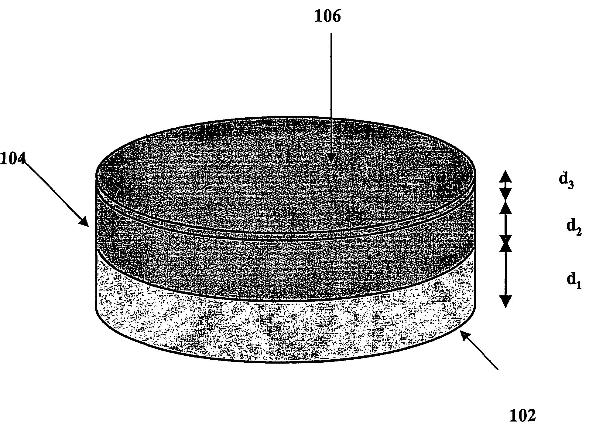
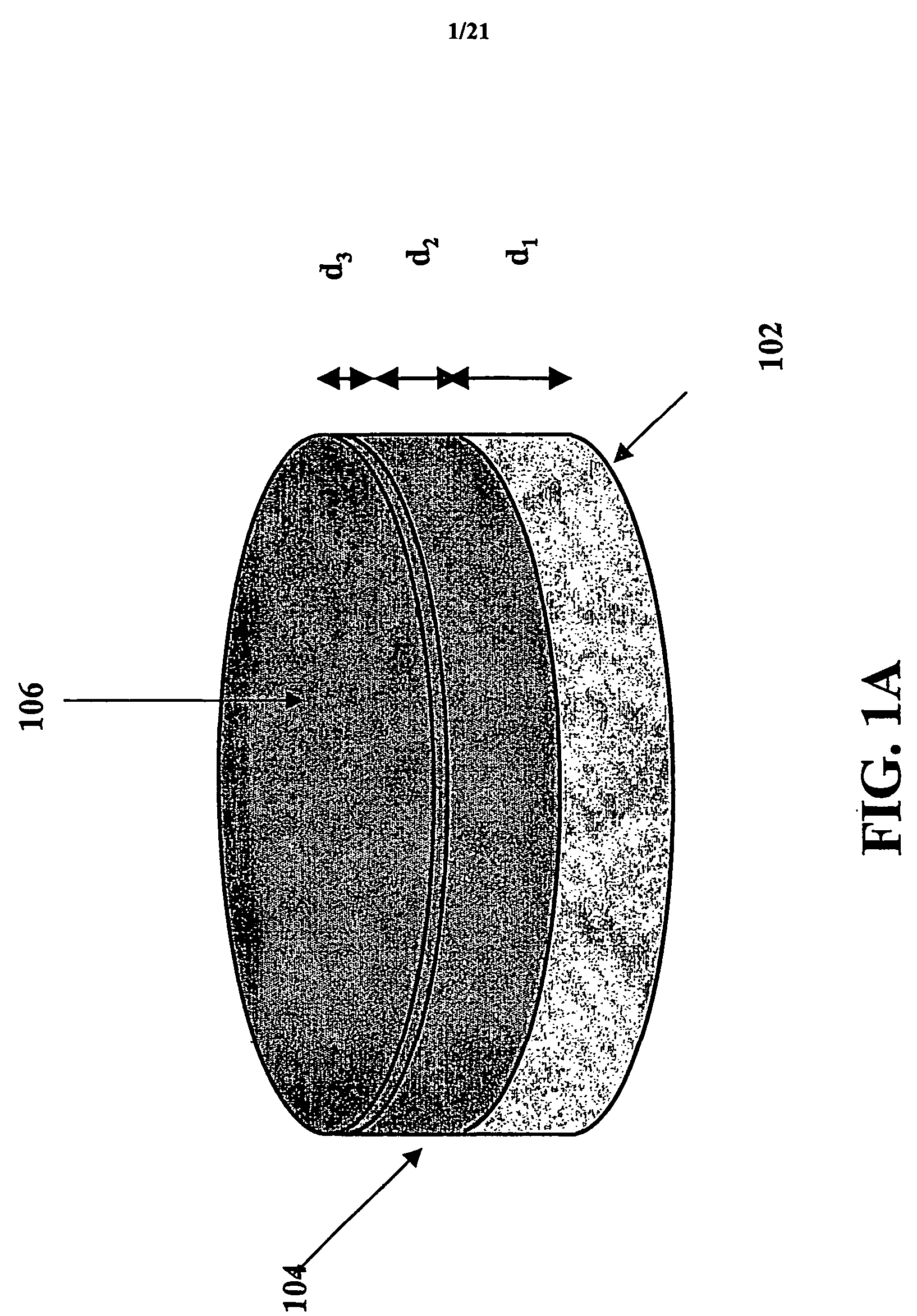
[0083] A ceramic-based, thin film optical microdetectors of this invention is represented schematically in FIG. 1A. The microdetector 100 is composed of biologically inert materials and includes a bottom electrode layer 102, where the layer is platinum, gold, or a conducting oxide such as LaSrCoO3, RuO2, doped CeO2, or IrO2 or mixtures thereof, an optically sensitive oxide layer 104 such as La doped PbZrTiO3 (PLZT) or other optically active perovskite. It is further contemplated that other doping elements for PbZrTiO3, including Sb, Mn, and Ca, can be used. Additionally, optically active oxides or nitrides such as ZnO, BiVMgO (BVM), GaN, or BN can be used. Optionally, the optical detector 100 may optionally include a top partially transparent conducting layer 106 as top electrode, where the this conductive layer is Pt, Au, LaSrCoO3 or other conducting oxide or mixtures...

example 2

[0089] This example illustrates the fabrication of individual optical devices from heterostructure of this invention.

[0090] Individual microdetectors or arrays of microdetectors are fabricated from the resultant heterostructure using negative photoresist lithography and ion milling as is standard in the microelectronics industry. The fabrication process is shown schematically in FIG. 4. In FIG. 4, the optically active heterostructure include a conductive layer 102 and a ceramic layer 104 on a substrate 108. Next, the heterostructure is covered by a uniform layer of negative photoresist by means of a spinner and baked on at 120° C. The micro-detector array is then patterned on the photoresist by using an appropriate pattern mask, e.g., an array of 40 micron diameter dots with 80 micron spacing, and the photoresist is exposed to UV light. The photoresist is then developed revealing a pattern of 40 micron dots of photoresist left at the surface of the heterostructure. The PLZT / Pt not ...

example 3

[0091] This example illustrates attaching the polymer membrane to an optical array of this invention.

[0092] After the detector arrays are photolithographically patterned on the MgO substrate, the polymer membrane is pressed onto the microdetectors for attachment to the membrane. Wet etching of the MgO substrate is then performed to remove the micro-detector array from the substrate, but leave the polymer carrier layer intact. The wet etching for an MgO substrate is performed in a ˜20% volume concentration of HCl for a period of 24 to 48 hours at room temperature. A dry etch process may also be performed to remove the substrate. This leaves the microdetectors attached to the polymer in their proper array, and with correct orientation and lateral placement for implant into the eye. FIG. 5A shows a TOD device with an 80 micron diameter microdetector and 160 micron spacing mounted on a PLGA polymer film used as a carrier and FIG. 5B shows a TOD device with a 200 micron square microdete...


PUM


Abstract

The present invention provides a method for capturing optical micro detectors for improved surgical handling during implantation into an eye comprising the steps of providing an optically active thin film heterostructure on a soluble substrate; forming an array comprising individual optical microdetectors from the optically active thin film heterostructure; attaching the optical microdetector array onto a biodegradable polymer carrier membrane; and separating the optical microdetector array attached to the biodegradable polymer carrier membrane from the soluble substrate thereby capturing the optical microdetectors in the bio-polymer carrier membrane for improved handling of the optical micro-detectors during transfer and implantation into the eye.

Description

BACKGROUND OF THE INVENTION [0001] 1. Field of the Invention [0002] The present invention relates to medical optically active implants to treat blindness and method for implanting these implants into an animal including a human to allow detection of visible light by the blind or to repair damaged areas of the retina to allow the animal to retain visual acuity in the damages areas. [0003] More particularly, the present invention relates to an implant including an array of optical microdetectors supported on or in a bio-absorbable substrate, where the microdetectors comprise a heterostructure. The present invention also relates to a method for making the implant, to a method for implanting the implant in an animal including a human and to methods for treating blindness, for replacing damaged retinal photo sensors and for ameliorating symptoms of diseases of the eye such as Retinitis Pigmentosa (RP) and Age-related Macular degeneration (AMD). [0004] 2. Description of the Related Art [0...

Claims


Application Information

Patent Timeline
Patent Type & Authority Applications(United States)
IPC IPC(8): A61F2/14A61F9/08A61N1/05A61N1/08A61N1/36
CPCA61F2/14A61F9/08A61N1/36046A61N1/08A61N1/0543
Inventor WU, NAIJUAN JZOMORRODIAN, ALI REZA
Owner UNIV HOUSTON SYST
Why Eureka
Try Eureka