Bath and method for high rate copper deposition

Inactive Publication Date: 2005-05-05
SEMITOOL INC
View PDF99 Cites 41 Cited by
  • Summary
  • Abstract
  • Description
  • Claims
  • Application Information

AI Technical Summary

Benefits of technology

[0008] The baths of the present invention are formulated to fully wet all the features on a workpiece, particularly the surface to be electroplated without having a substantial adverse effect on the ability of the brightener to reduce the size of the metal grains and make the surface of the deposit brighter. The bath wets all features on the workpiece so that bubble trapping, pore formation, a

Problems solved by technology

One of the shortcomings of this commercial technology is that a copper deposition rate of 0.4-1.0 μm per minute is undesirably slow, not only for bumping applications, but for other through-mask plating applications requiring relatively thick deposits, e.g., micron

Method used


Image

  • Bath and method for high rate copper deposition
  • Bath and method for high rate copper deposition
  • Bath and method for high rate copper deposition

Examples


Embodiment Construction

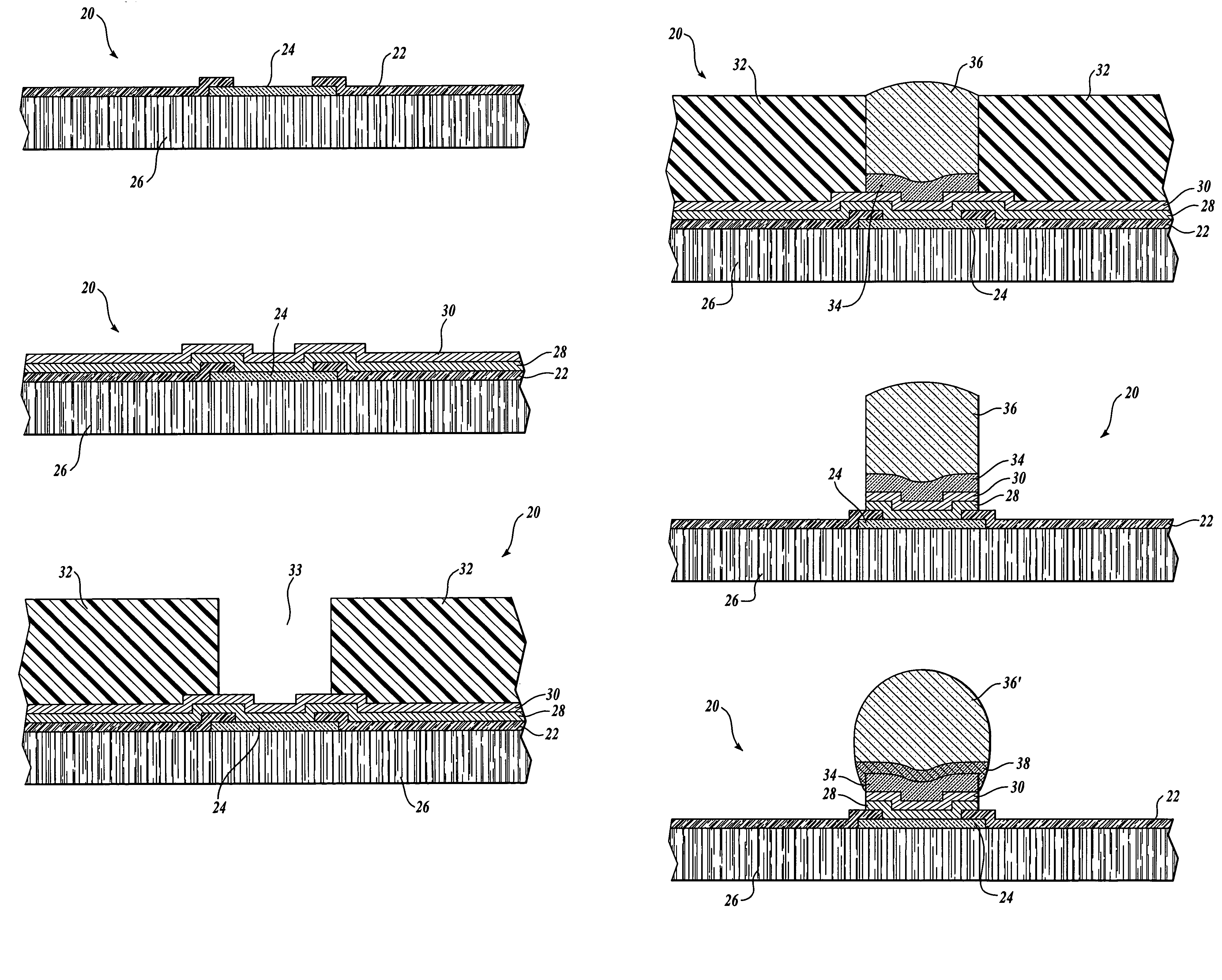
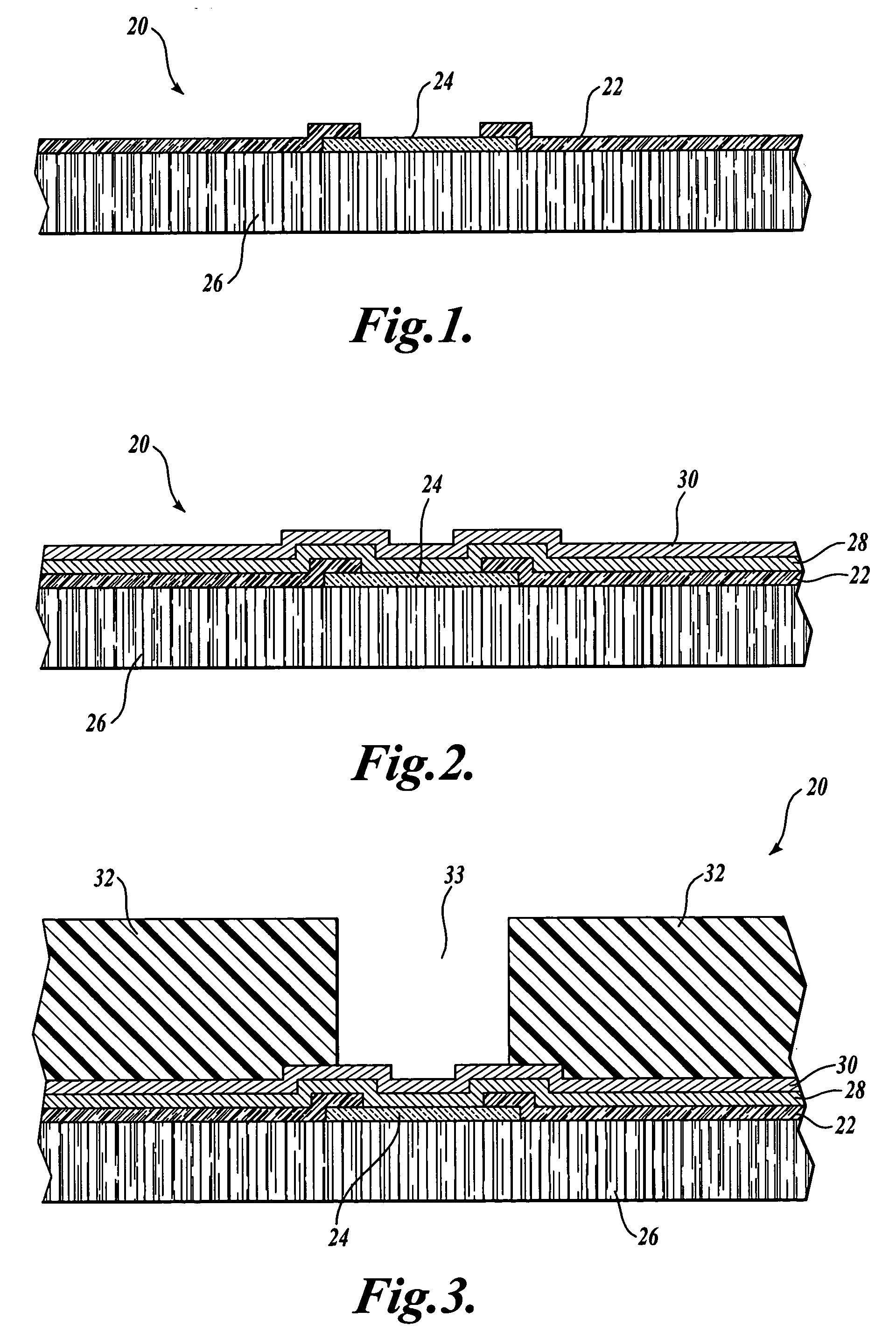
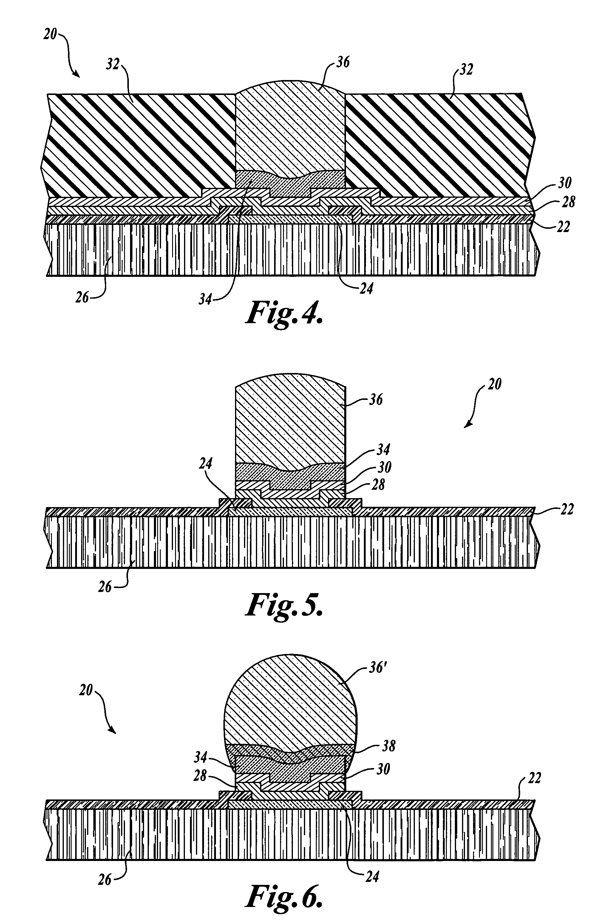
[0022] As used throughout the specification, the following abbreviations have the following meanings, unless the context clearly indicates otherwise: nm=nanometers, mm=millimeters, μm=microns, μm / min=microns per minute, g / L=grams per liter, ml / L=milliliters per liter, mA / cm2=milliamperes per square centimeter, and ppm=parts per million. All percentages and ratios are by weight unless otherwise indicated. All ranges are inclusive and combinable.

[0023] As used throughout the specification, the term “plating” refers to electrolytic deposition, i.e., electroplating, unless the context clearly indicates otherwise. The term “feature” refers to a structure on a substrate. The term “through-mask plating” refers to plating through an opening in a dielectric film, such as a photoresist. The term “through-hole and blind hole plating” refers to plating through an opening in a material, which is not a photoresist. The term “brightener” refers to an organic compound that reduces the size of the ...


PUM

PropertyMeasurementUnit
Temperatureaaaaaaaaaa
Fractionaaaaaaaaaa

Abstract

A plating bath for electroplating copper on a microelectronic workpiece in a through-mask plating application at a rate of at least 2 μm/min where the bath includes: (a) 50-85 g/L of Cu2+; (b) 50-100 g/L of H2SO4; (c) 30-150 ppm of Cl—; (d) a brightener; (e) a wetting agent; (f) optionally a leveler; and (g) water. A process for electroplating copper on a microelectronic workpiece in a through-mask plating application at a rate of at least 2 μm/min where the process includes the steps of: (a) providing the plating bath described above; (b) providing a workpiece which has one or more through-mask openings having a conductive layer at the bottom of the openings; (c) contacting the conductive layer with the plating bath; and (d) providing electroplating power between the conductive layer and an anode disposed in electrical contact with the bath, whereby copper is deposited onto the conductive layer at a rate of at least 2 μm/min.

Description

FIELD OF THE INVENTION [0001] The invention is in the field of electroplating copper on a microelectronic workpiece using a plating bath. More particularly, the invention relates to electroplating copper on a microelectronic workpiece in a plating bath wherein the copper is deposited at a high rate in a through-mask plating application. BACKGROUND OF THE INVENTION [0002] Copper electroplating uses the process of electrolysis to deposit copper atoms on an object acting as the cathode, or negative electrode. Applications of electroplating of copper on microelectronic substrates in a plating bath can be divided into several categories, such as interconnect plating applications, micro-electro-mechanical systems (MEMS) plating applications, and bump plating applications. These pattern plating applications can be mainly divided into through-mask plating applications (photoresist pattern plating applications such as bump applications, MEMS applications, and redistribution applications) and...

Claims


Application Information

Patent Timeline
IPC IPC(8): C25D3/38C25D5/02C25D5/18H01L21/288H01L21/60
CPCC25D3/38C25D5/022H01L2924/0002H01L2224/0401H01L2924/014H01L2924/01033H01L2924/01024H01L2924/01021H01L2924/01019H01L2924/01006H01L2924/01005H01L2924/00013C25D5/18H01L21/2885H01L24/11H01L2224/03912H01L2224/05568H01L2224/05572H01L2224/11462H01L2224/1147H01L2224/11849H01L2224/11912H01L2224/13023H01L2224/1308H01L2224/13083H01L2224/131H01L2224/13147H01L2924/01011H01L2924/01013H01L2924/01016H01L2924/01022H01L2924/01029H01L2924/01047H01L2924/01078H01L2924/01082H01L2924/01088H01L2924/01322H01L2924/01327H01L2924/19042H01L2924/00014H01L2224/13099H01L2224/05552C25D5/611C25D5/617H01L24/05H01L2224/0347H01L2224/0361H01L2224/03914H01L2224/05124H01L2224/05147H01L2224/05166H01L2224/05171H01L2224/05647H01L2924/12044H01L2924/00H01L2924/01074H01L2924/013
Inventor KIM, BIOHGIBBONS, KENNETH W.
Owner SEMITOOL INC
Why Eureka
Try Eureka