[0007] To address or solve the above and / or other problems, exemplary embodiments of the present invention provide a method to form a patterned conductive film, including irradiating with light a substrate that is provided with a conductive layer including a conductive material and includes a photothermal conversion material that converts
light energy into
heat energy to fire at least part of the conductive layer with the photothermal conversion material. According to exemplary embodiments of the present invention, the substrate, including the photothermal conversion material, can efficiently convert the
light energy of the emitted light into
heat energy. The substrate can therefore supply the conductive layer with sufficient heat energy to fire the conductive layer to develop its
conductivity. According to exemplary embodiments of the present invention, additionally, the photothermal conversion material is irradiated with light to generate instantaneous
high heat, thereby firing the conductive layer in a short time. According to exemplary embodiments of the present invention, furthermore, the substrate is instantaneously supplied with heat energy. Even if, for example, the substrate is composed of a material having no
heat resistance, such as a plastic, the effect on the substrate can be reduced or suppressed. In the method to form a patterned conductive film according to exemplary embodiments of the present invention, a predetermined region of the substrate may be irradiated with light to pattern the conductive layer, thereby forming a conductive film having a pattern according to the irradiated region on the substrate.
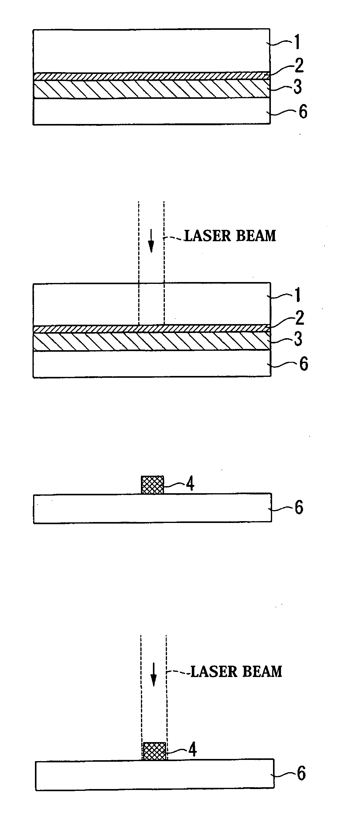
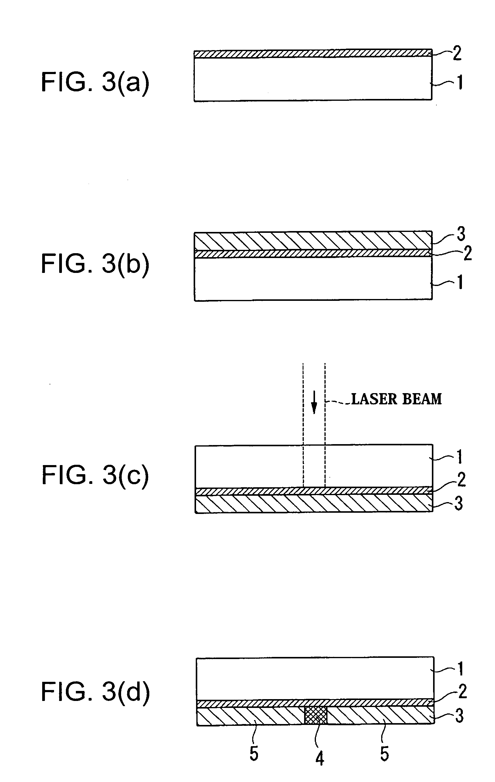
[0009] In the method to form a patterned conductive film according to exemplary embodiments of the present invention, a photothermal conversion layer including the photothermal conversion material may be independently provided on the substrate such that the photothermal conversion layer and the conductive layer are adjacent on the substrate. Alternatively, the photothermal conversion material may be mixed in the substrate. In either manner, the heat energy generated by the photothermal conversion material can be supplied to the conductive layer to fire the conductive layer. In particular, the heat energy generated in the photothermal conversion layer can be efficiently supplied to the conductive layer if the photothermal conversion layer and the conductive layer are adjacent.
[0012] In the method to form a patterned conductive film according to exemplary embodiments of the present invention, a patterned conductive film may be formed on a predetermined board by bringing the board into contact with the conductive layer on the substrate and irradiating a predetermined region of the substrate with light to transfer the part of the conductive layer corresponding to the predetermined region onto the board. That is, the patterned conductive film, which is formed on the substrate, may be transferred onto a predetermined board by irradiation with light. Then the patterned conductive film transferred onto the board may be further irradiated with light, thereby reliably firing the patterned conductive film on the board to develop its
conductivity.
[0013] In the method to form a patterned conductive film according to exemplary embodiments of the present invention, the light may be a laser beam, and the irradiation may be performed with light having a
wavelength according to the photothermal conversion material. The photothermal conversion material can efficiently convert the light energy of such light into heat energy.
[0014] In the method to form a patterned conductive film according to exemplary embodiments of the present invention, the irradiation may be performed through a
mask having a predetermined pattern to irradiate the substrate with light passing through the
mask. The
mask enables the formation of a conductive film having a pattern finer than the
beam diameter of the light emitted. Alternatively, the irradiation may be performed while relatively moving the substrate with respect to the light. That is, the light (laser beam) and the substrate may be relatively moved to pattern the conductive layer. This manner can eliminate a step of preparing the mask.
[0015] Exemplary embodiments of the present invention provide an electrooptical device including a patterned conductive film formed by the above method and an electronic appliance including the electrooptical device. According to exemplary embodiments of the present invention, the electrooptical device and the electronic appliance including the electrooptical device can be manufactured with
high productivity and have desirable performance. Examples of the electrooptical device include
liquid crystal displays, organic electroluminescent (EL) displays, and
plasma displays.

