Method of fabricating vertical structure LEDs

a technology of leds and vertical structures, applied in the direction of resistors, semiconductor devices, solid-state devices, etc., can solve the problems of high cost of manufacturing gan-based devices, difficult to dice sapphire substrates, and too expensive gan devices for many applications

Inactive Publication Date: 2005-05-12
SUZHOU LEKIN SEMICON CO LTD
View PDF64 Cites 59 Cited by
  • Summary
  • Abstract
  • Description
  • Claims
  • Application Information

AI Technical Summary

Benefits of technology

[0019] The principles of the present invention provide for a method of fabricating semiconductor devices on insulating substrates by first forming semiconductor layers on the insulating substrate, followed by forming a metal layer over the semiconductor layers, followed by removal of the insulating substrate to isolate a structurally supported wafer comprised of the formed semiconductor layers and the metal layer. The metal layer supports the semiconductor layers to prevent warping and / or other damage and provides for electrical contacts. Beneficially, the metal layer includes a metal, such as Cu, Cr, Ni, Au, Ag, Mo, Pt, Pd, W, or Al, or a metal containing material such as titanium nitride. Forming of the metal layer can be performed in numerous ways, for example, by electroplating, by electro-less plating, by CVD, or by sputtering. Subsequently, bottom electrical contacts can be added to the semiconductor layers and then individual semiconductor devices can be diced from the resulting structure.

Problems solved by technology

Despite the rapid development of GaN device technology, GaN devices are too expensive for many applications.
One reason for this is the high cost of manufacturing GaN-based devices, which in turn is related to the difficulties of growing GaN epitaxial layers and of subsequently dicing out completed GaN-based devices.
However, since sapphires are extremely hard, are chemically resistant, and do not have natural cleave angles, sapphire substrates are difficult to dice.
It should be noted that such mechanical steps are time consuming and expensive, and that such steps reduce device yields.
Even after thinning sapphires remain difficult to dice.
Such scribing typically requires at least half an hour to process one substrate, adding even more to the manufacturing costs.
Additionally, since the scribe lines have to be relatively wide to enable subsequent dicing, the device yields are reduced, adding even more to manufacturing costs.
Such mechanical handling reduces yields even more.
Of note, because sapphire is an insulator the LED device topologies that are available when using sapphire substrates (or other insulating substrates) are, in practice, limited to lateral and vertical topologies.
Furthermore, plasma damage to the GaN step surface is often sustained during the dry-etch process.
Such closely spaced electrodes 34 are highly susceptible to ESD damage.
Such removal can be difficult, particularly if device yields are of concern.
Thus, to provide the same amount of light emission area, lateral GaN-based LEDs must have a larger surface area, which lowers device yields.
Furthermore, the lateral topology is more vulnerable to static electricity, primarily because the two electrodes (36 and 40) are so close together.
Additionally, as the lateral topology is fabricated on an insulating substrate, and as the vertical topology can be attached to a heat sink, the lateral topology has relatively poor thermal dissipation.
This is primarily because of the difficulties of removing the insulating substrate and of handling the GaN wafer structure without a supporting substrate.
But, substrate removal and subsequent wafer bonding of large area wafers remains very difficult due to inhomogeneous bonding between the GaN wafer and the 2nd (substitutional) substrate.

Method used


Image

  • Method of fabricating vertical structure LEDs
  • Method of fabricating vertical structure LEDs
  • Method of fabricating vertical structure LEDs

Examples


Embodiment Construction

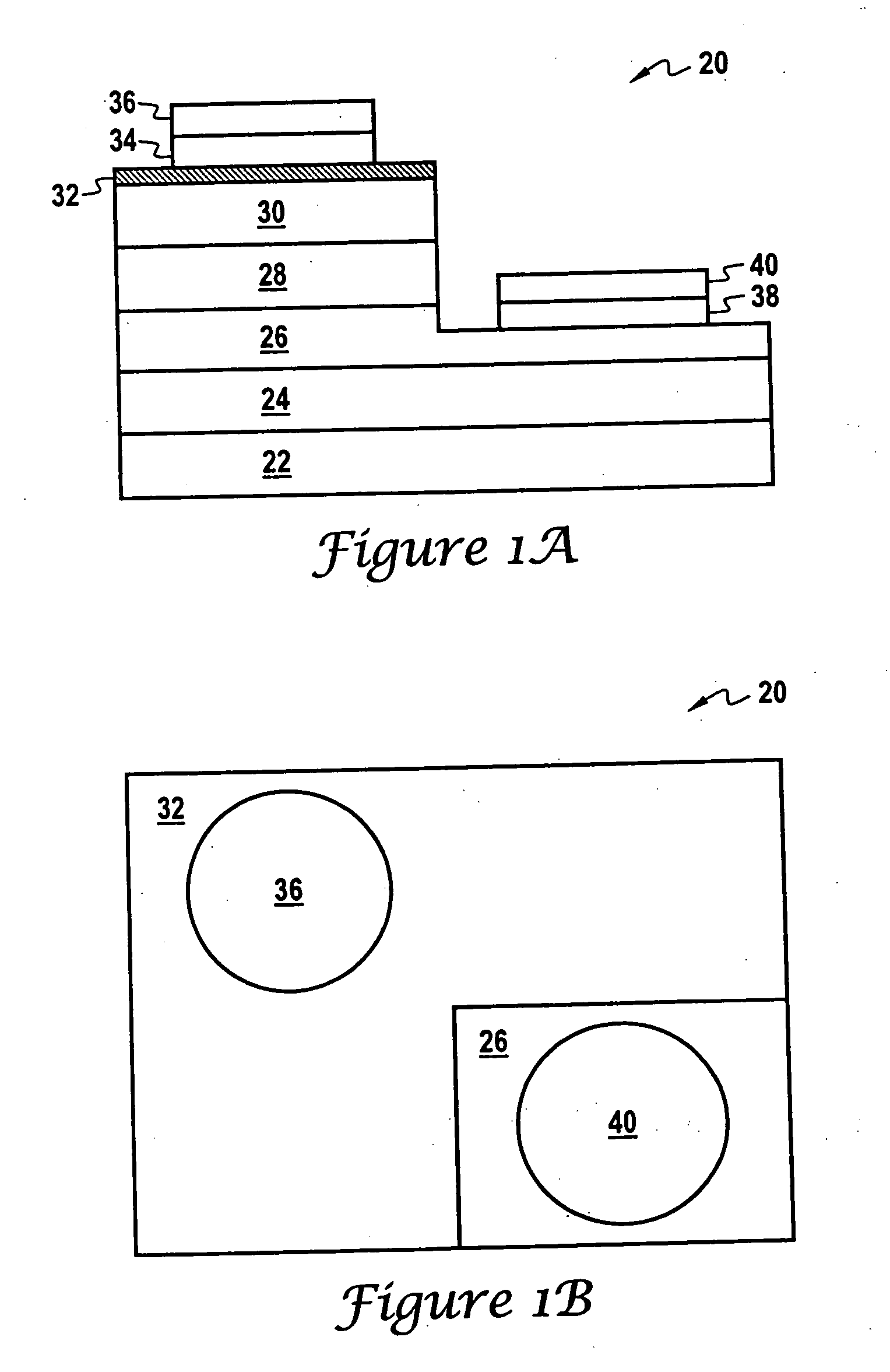
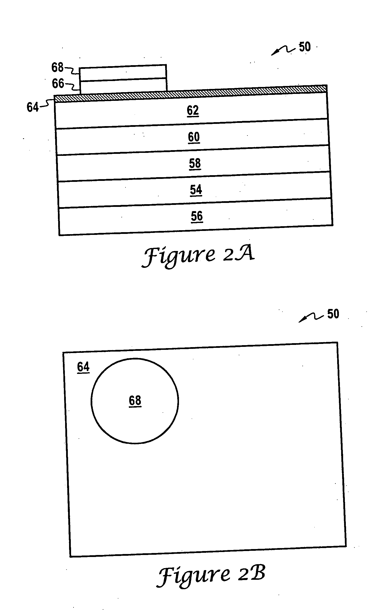
[0030] The principles of the present invention provide for methods of fabricating semiconductor devices, such as GaN-based vertical topology LEDs, on insulating substrates, such as sapphire substrates, using metal support films. While those principles are illustrated in a detailed description of a method of fabricating vertical topology GaN-based LEDs on a sapphire substrate, those principles are broader than that illustrated method. Therefore, the principles of the present invention are to be limited only by the appended claims as understood under United. States Patent Laws.

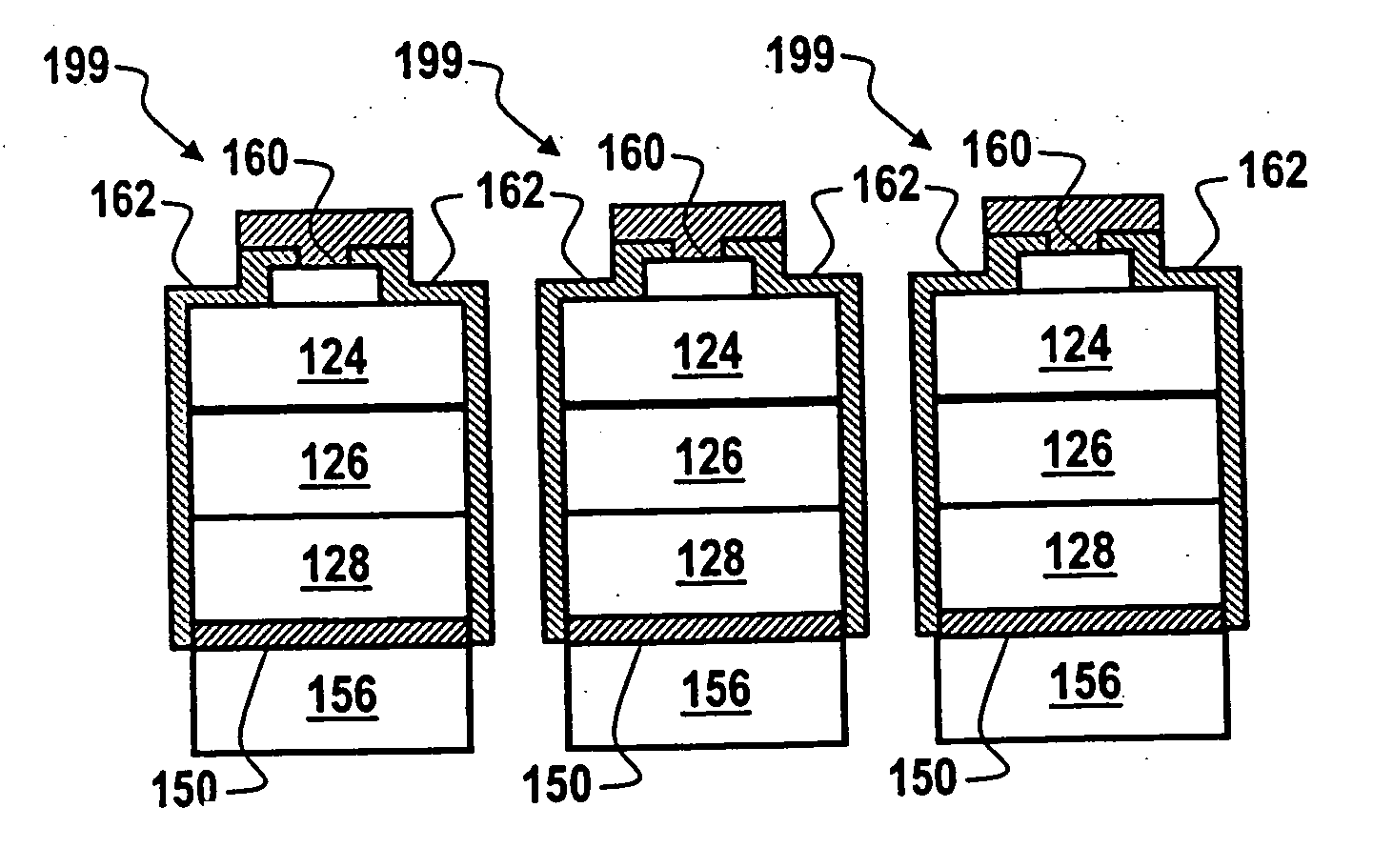
[0031]FIGS. 3-15 illustrate a method of manufacturing vertical topology GaN-based light emitting diodes (LEDs) on sapphire substrates. Sapphire substrates are readily available in suitable sizes, are thermally, chemically, and mechanically stable, are relatively inexpensive, and support the growth of good quality GaN epitaxial layers. It should be understood that those figures are not to scale.

[0032] Referring...


PUM


Abstract

A method of fabricating semiconductor devices, such as GaN LEDs, on insulating substrates, such as sapphire. Semiconductor layers are produced on the insulating substrate using normal semiconductor processing techniques. Trenches that define the boundaries of the individual devices are then formed through the semiconductor layers and into the insulating substrate, beneficially by using inductive coupled plasma reactive ion etching. The trenches are then filled with an easily removed layer. A metal support structure is then formed on the semiconductor layers (such as by plating or by deposition) and the insulating substrate is removed. Electrical contacts, a passivation layer, and metallic pads are then added to the individual devices, and the individual devices are then diced out.

Description

BACKGROUND OF THE INVENTION [0001] 1. Field of the Invention [0002] The present invention relates to semiconductor device fabrication. More particularly, the present invention relates to a method of fabricating vertical devices using a metal support layer. [0003] 2. Discussion of the Related Art [0004] Light emitting diodes (“LEDs”) are well-known semiconductor devices that convert electrical current into light. The color (wavelength) of the light that is emitted by an LED depends on the semiconductor material that is used to fabricate the LED. This is because the wavelength of the emitted light depends on the semiconductor material's band-gap, which represents the energy difference between the material's valence band and conduction band electrons. [0005] Gallium-Nitride (GaN) has gained much attention from LED researchers. One reason for this is that GaN can be combined with indium to produce InGaN / GaN semiconductor layers that emit green, blue, and white light. This wavelength con...

Claims


Application Information

Patent Timeline
Patent Type & Authority Applications(United States)
IPC IPC(8): H01C7/00H01L21/02H01L27/08H01L33/00H01L33/32H01L33/44
CPCH01C7/006H01C7/008H01L27/0802H01L28/20H01L33/0079H01L33/32H01L33/62H01L33/38Y10S438/958Y10S438/977H01L33/0025H01L33/06H01L33/40H01L33/44H01L33/0093H01L33/36H01L33/007H01L33/0095H01L33/12
Inventor LEE, JONG-LAMJEONG, IN-KWONYOO, MYUNG CHEOL
Owner SUZHOU LEKIN SEMICON CO LTD
Why Eureka
Try Eureka