Semiconductor device including an improved capacitor and method for manufacturing the same

Inactive Publication Date: 2005-05-12
SAMSUNG ELECTRONICS CO LTD
View PDF1 Cites 24 Cited by
  • Summary
  • Abstract
  • Description
  • Claims
  • Application Information

AI Technical Summary

Benefits of technology

[0018] According to some embodiments of the invention, a capacitor may have an improved structural stability

Problems solved by technology

As a result, adjacent capacitors having high aspect ratios may lean against each other, causing them to become electrically connected and generating a two-bit short between the adjacent capacitors.
Thus, cost and ti

Method used


Image

  • Semiconductor device including an improved capacitor and method for manufacturing the same
  • Semiconductor device including an improved capacitor and method for manufacturing the same
  • Semiconductor device including an improved capacitor and method for manufacturing the same

Examples


Embodiment Construction

[0026] The invention will be described more fully below with reference to the accompanying drawings.

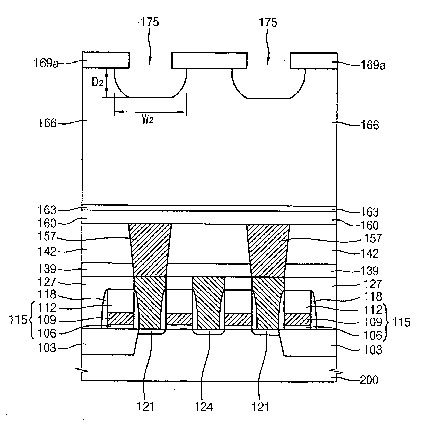
[0027]FIGS. 2A and 2B are cross-sectional diagrams that illustrate processes for forming first pads 121 and second pads 124 on a semiconductor substrate 100 including word lines 130.

[0028] Referring to FIGS. 2A and 2B, an isolation layer 103 is formed at a surface portion of a substrate 100 to define an active region and a field region on the substrate 100. The isolation layer 103 may be formed via a shallow trench isolation (STI) process or a local oxidation of silicon (LOCOS) process.

[0029] A thin gate oxide layer (not shown) is formed on the substrate 100 by a thermal oxidation process or a chemical vapor deposition (CVD) process. Here, the gate oxide layer is formed only on the active region defined by the isolation layer 103.

[0030] A first conductive layer (not shown) and a first mask layer (not shown) are formed successively on the gate oxide layer. The first conductive laye...


PUM


Abstract

In a semiconductor device according to embodiments of the invention, a capacitor includes a storage electrode having a cylindrical storage conductive layer pattern and connecting members formed on the upper portion of the cylindrical storage conductive layer pattern. The connecting member connects to an adjacent connecting member of another storage electrode. A dielectric layer and a plate electrode are successively formed on the storage electrode. All of the capacitors are connected by one another by forming cylindrical storage electrodes so that the storage electrode does not fall down when the capacitors have an extremely large aspect ratio. Thus, the capacitance of the capacitors may be improved to the desired level. A semiconductor device that includes these capacitors may have improved reliability and the throughput of a semiconductor manufacturing process may be increased.

Description

CROSS REFERENCE TO RELATED APPLICATIONS [0001] This application is a Continuation-In-Part application of U.S. patent application Ser. No. 10 / 916,672, which was filed on 11 Aug. 2004. This application claims priority from U.S. patent application Ser. No. 10 / 916,672 as well as from Korean Patent Application No. 2003-86462, filed on 1 Dec. 2003, the contents of which are herein incorporated by reference in their entirety for all purposes.BACKGROUND OF THE INVENTION [0002] 1. Field of the Invention [0003] This disclosure relates to semiconductor devices, and more particularly to a semiconductor device that includes a capacitor having an improved structural stability and an enhanced capacitance, and a method of manufacturing the semiconductor device. [0004] 2. Description of the Related Art [0005] In general, semiconductor memory devices such as dynamic random access memory (DRAM) devices can store data or information therein. The data or information may be stored to as well as read out ...

Claims


Application Information

Patent Timeline
IPC IPC(8): H01L21/02H01L21/311H01L21/768H01L21/8242H01L27/02H01L27/108
CPCH01L21/31116H01L21/76802H01L27/0207H01L28/91H01L27/10817H01L27/10852H01L27/10855H01L27/10814Y10S257/906H10B12/318H10B12/315H10B12/033H10B12/0335
Inventor PARK, JE-MIN
Owner SAMSUNG ELECTRONICS CO LTD
Why Eureka
Try Eureka