High temperature laser diode

a laser diode, high temperature technology, applied in the direction of lasers, laser details, electrical equipment, etc., can solve the problems of increasing cost, complexity, power dissipation, and inability to meet the requirements of applications beyond 1.2 m, and achieve the effect of low power dissipation

Inactive Publication Date: 2005-05-12
NORTEL NETWORKS UK
View PDF15 Cites 4 Cited by
  • Summary
  • Abstract
  • Description
  • Claims
  • Application Information

AI Technical Summary

Benefits of technology

[0047] The laser structure can operate at high temperatures and is very useful for coolerless operation required for low power dissipation in optical systems.

Problems solved by technology

Gallium arsenide (GaAs) based material systems are well suited to short wavelength applications and present excellent high temperature performance but they are generally not suited to applications beyond about 1.2 μm.
InP material systems usually exhibit poor high temperature performance, thus in order to operate InP based devices reliably, external cooling is usually required.
It is well known in the art to package semiconductor laser diodes with integral thermoelectric coolers which increase cost, complexity and power dissipation.
Conversely, the poor temperature performance in typical InP material systems is usually attributed to the small conduction band offset, which is also often due to the lack of a suitable available material with a higher energy bandgap and a lower index of refraction than InP.
However, it is not necessarily suitable or desirable to use the GaAs system, especially for optical telecommunications wavelengths.
The above described prior art laser structures have poor temperature performance or other disadvantages.

Method used


Image

  • High temperature laser diode
  • High temperature laser diode
  • High temperature laser diode

Examples


first embodiment

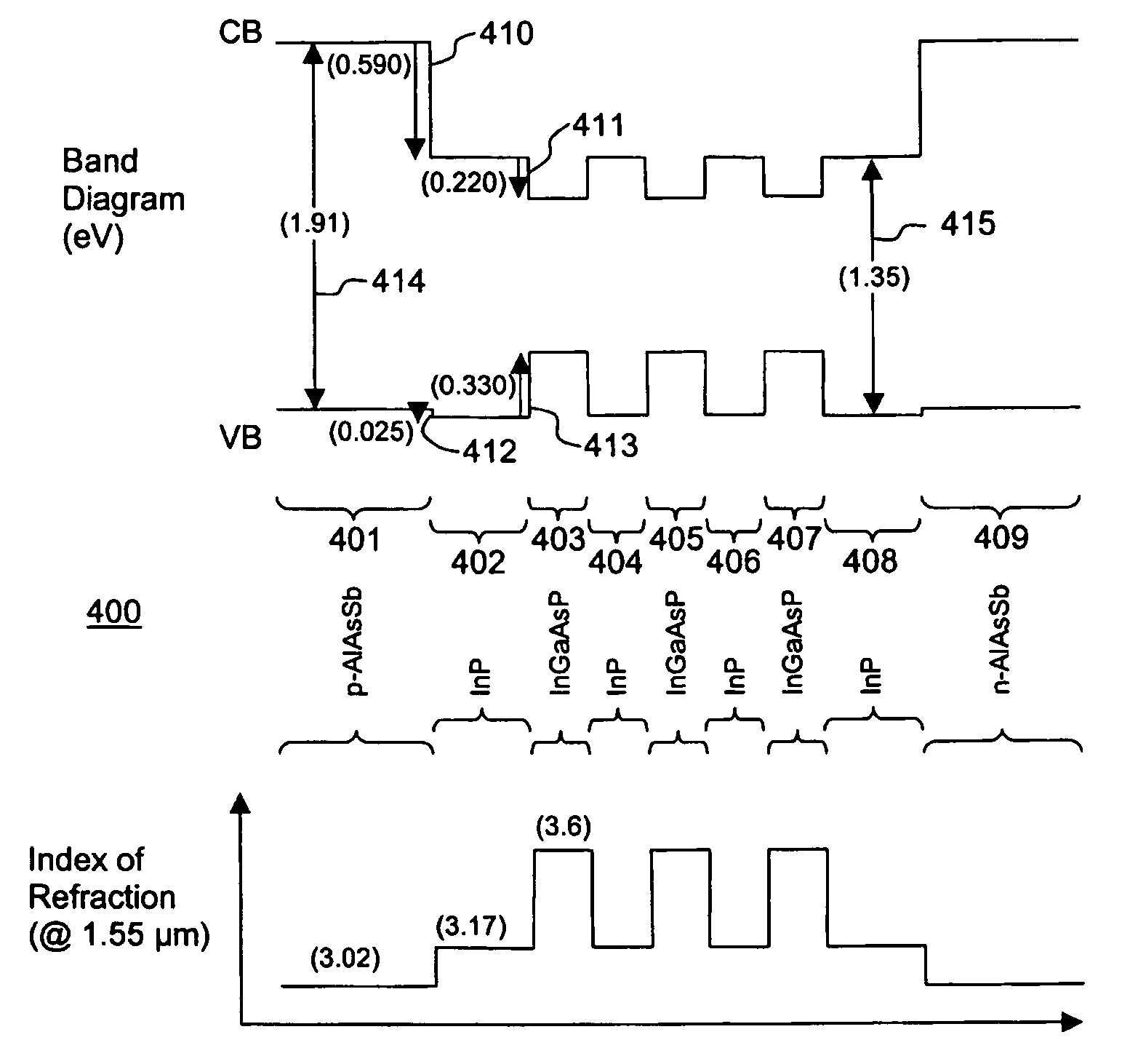
[0058]FIG. 4 illustrates the semiconductor laser structure of the present invention. This laser uses a InP material system traditionally used for telecommunications systems but with novel AlAsSb waveguide cladding layers. Referring to FIG. 4, the laser structure 400 comprises an active region comprising quantum wells 403, 405, 407 of InGaAsP and separated by barrier layers 404, 406 of InP. The active region is bounded by confinement layers 402, 408. The confinement layers 402, 408 are bounded respectively by cladding layer 401 of p-AlAsSb and cladding layer 409 of n-AlAsSb. These layers are deposited on a InP substrate (not shown). Referring to the band diagram of FIG. 4, the conduction band offset 410 between the cladding layers (401, 409) and the confinement layers (402, 408) is 594 meV. The conduction band offset 411 between the confinement and barrier layers (402, 404, 406, 408) and the quantum wells (403, 405, 407) is 220 meV. The valence band offset 412 between the cladding la...

second embodiment

[0061]FIG. 5 illustrates the semiconductor laser structure of the present invention using a newer material system than that of the embodiment of FIG. 4, and exhibits better high temperature performance. This laser uses AlAsSb waveguide cladding layers with InAlAs barriers and InGaAlAs quantum wells. Referring to FIG. 5, the laser structure 500 comprises an active region comprising quantum wells 503, 505, 507 of InGaAlAs, separated by barrier layers 504, 506 of InAlAs. The active region is bounded by confinement layers 502, 508. The confinement layers 502, 508 are bounded respectively by cladding layer 501 of p-AlAsSb and cladding layer 509 of n-AlAsSb. Referring to the band diagram of FIG. 5, the conduction band offset 510 between the cladding layers (501, 509) and the confinement layers (502, 508) is about 334 meV. The conduction band offset 511 between the confinement and barrier layers (502, 504, 506, 508) and the quantum wells (503, 505, 507) is 462 meV. The valence band offset ...


PUM


Abstract

A semiconductor laser structure having confinement layers to confine electrons to an active region (quantum wells) and having separate antimonide-based cladding layers to provide additional electron confinement and photon confinement is suited to high temperature operation. The structure is suitable for lasing across telecommunications wavelengths from 980 nm to 1.55 μm (microns). The cladding layer uses AlAsSb which can be lattice-matched to InP and can be used to achieve large conduction band offsets. It is very useful for coolerless (without thermo-electric cooler) operation.

Description

CROSS REFERENCE TO RELATED APPLICATIONS [0001] This application claims priority from U.S. Provisional Patent application Ser. No. 60 / 517,400 filed Nov. 6, 2003.MICROFICHE APPENDIX [0002] Not Applicable. TECHNICAL FIELD [0003] The present invention relates to semiconductor laser diodes and in particular, to a semiconductor laser diode which has excellent temperature characteristics. BACKGROUND OF THE INVENTION [0004] Semiconductor laser diodes can be divided into two groups, those for use in short wavelength applications (λ=0.78-0.89 μm) (1 μm=1 micron) and those for use in long wavelength applications (λ=0.98-1.6 μm). Gallium arsenide (GaAs) based material systems are well suited to short wavelength applications and present excellent high temperature performance but they are generally not suited to applications beyond about 1.2 μm. However, modern optical telecommunications systems operate at long wavelengths, typically 980 nm to 1.55 μm and thus indium-phosphide (InP) based materia...

Claims


Application Information

Patent Timeline
Patent Type & Authority Applications(United States)
IPC IPC(8): H01S5/00H01S5/20H01S5/30H01S5/32H01S5/343
CPCB82Y20/00H01S5/2009H01S5/3211H01S5/3438H01S5/34313H01S5/3434H01S5/34346H01S5/34306
Inventor REID, BENOIT
Owner NORTEL NETWORKS UK
Why Eureka
Try Eureka