Vertical impedance sensor arrangement and method for producing a vertical impedance sensor arrangement

a technology of vertical impedance sensor and impedance sensor, which is applied in the direction of instruments, specific use bioreactors/fermenters, biomass after-treatment, etc., can solve the problems of complex preparation, easy errors in marking capture molecules with fluorescent labels, and low detection sensitivity of fluorescent labels

Inactive Publication Date: 2005-05-12
SIEMENS AG
View PDF10 Cites 54 Cited by
  • Summary
  • Abstract
  • Description
  • Claims
  • Application Information

AI Technical Summary

Benefits of technology

[0035] The invention is based on the problem of providing a sensor arrangement for detecting particles by means of the particles hybridizing with immobilized capture molecules, which sensor arrangement has an improved detection sensitivity.
[0039] In the case of the vertical impedance sensor arrangement according to the invention, the distance between the sensor electrodes, that is to say the first and second electrically conductive structures, is defined by means of a vertical arrangement. By depositing a layer as a spacer, it is possible to set the distance between the electrodes with a very high accuracy. A fundamental idea of the invention is to be seen in the fact that a thickness of the spacer is prescribed by means of a deposition method, and not using a patterning method as in the prior art. Appropriate deposition methods are, in particular, an atomic layer deposition method or a chemical vapor phase epitaxy method. Particularly in the case of the atomic layer deposition method (ALD method), it is possible to set the accuracy of a deposited layer down to an accuracy of as much as one atomic layer, that is to say down to an accuracy of a few angstroms. Therefore, it is possible to set a distance between the sensor electrodes of a sensor arrangement with a very high accuracy. A minimum distance between the two sensor electrodes of less than 100 nm can therefore be achieved without any problems.
[0040] Using the effect explained with reference to FIG. 3A, FIG. 3B, in the case of a reduced distance between the sensor electrodes, the electric field distribution between the sensor electrodes is influenced to a particularly great extent by a hybridization event. As a result, the detection sensitivity of the vertical impedance sensor arrangement according to the invention is significantly increased compared with the prior art. Moreover, the vertical impedance sensor arrangement according to the invention can be produced by means of a simple lithography and a simple lift-off method. Therefore, the production of the vertical impedance sensor arrangement can be realized with a low outlay.
[0049] The capture molecules are often very expensive biological molecules that are difficult to obtain and are often present only in a small quantity. By virtue of a part of the uncovered surface sections of the electrically conductive structures being covered by means of a protective layer or by means of an encapsulation, specific surface regions on which capture molecules are immobilized can be prescribed in a targeted manner. The number of capture molecules required is thereby reduced.

Problems solved by technology

However, spectroscopic methods in which the intensity of a fluorescent radiation or an electromagnetic radiation intensity that is attenuated on account of an absorption of radiation is detected are complicated and often difficult in terms of preparation.
Furthermore, marking capture molecules with fluorescent labels is susceptible to errors.
Devices for generating or for detecting electromagnetic radiation are expensive and complicated.
The known impedance methods have the disadvantage that an electrical signal that is only very small in each case can be evaluated.
However, it is technologically difficult to produce spacings of less than 200 nm using a lithography method.
This requires a very expensive, demanding lithography.
On account of fundamental physical restrictions such as undesirable diffraction phenomena in the case of optical lithography with a mask having a very small dimension or on account of the relatively high inaccuracy in the case of a lithographic patterning (errors of 20 nm or worse), it is extremely difficult to form a sensor arrangement with electrodes having a sufficiently small dimension which are produced using a patterning method.

Method used


Image

  • Vertical impedance sensor arrangement and method for producing a vertical impedance sensor arrangement
  • Vertical impedance sensor arrangement and method for producing a vertical impedance sensor arrangement
  • Vertical impedance sensor arrangement and method for producing a vertical impedance sensor arrangement

Examples


Embodiment Construction

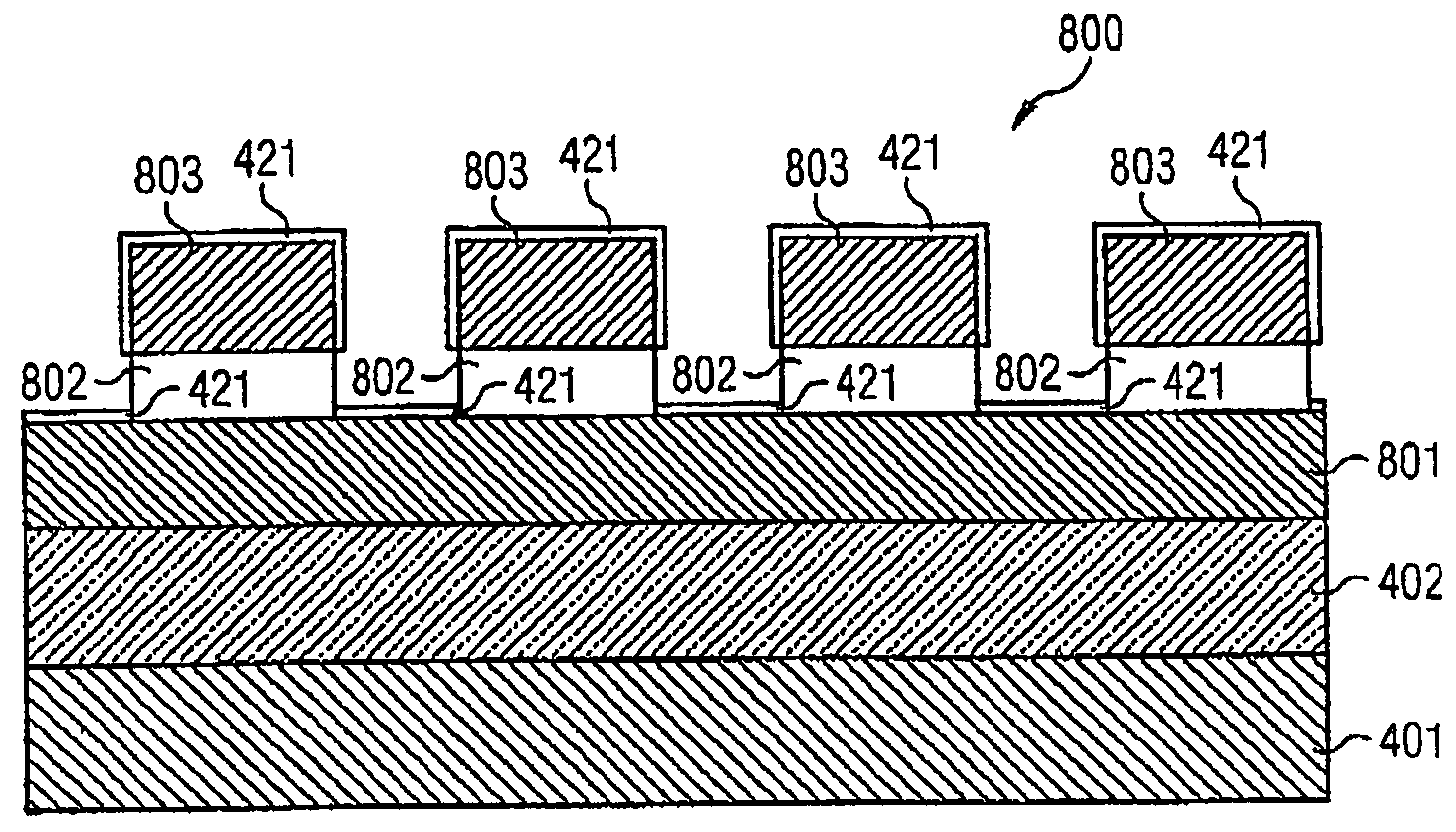
[0076] It should be noted that in the description of the exemplary embodiments, those components of vertical impedance sensor arrangements which are included in different exemplary embodiments are provided with identical reference numerals.

[0077] A description is given below, with reference to FIG. 4A to 4C, of an exemplary embodiment of the method according to the invention for producing a vertical impedance sensor arrangement.

[0078] In order to obtain the layer sequence 400 shown in FIG. 4A, a passivation layer 402 made of silicon nitride is deposited on a silicon wafer 401. Furthermore, a gold layer is deposited on the passivation layer 402 using a vapor deposition method and is patterned using a photolithography method (e.g. lift-off method). As a result, a first gold conductor track 403 and a second gold conductor track 404 remain on the passivation layer 402. A silicon dioxide layer 405 is subsequently deposited on the surface of the layer sequence thus obtained, using a CVD...


PUM

PropertyMeasurementUnit
distanceaaaaaaaaaa
distanceaaaaaaaaaa
distanceaaaaaaaaaa

Abstract

Vertical impedance sensor arrangement including a substrate, a first electrically conductive structure having a first uncovered surface and being arranged in and / or on the substrate, a spacer arranged above the substrate and / or at least partially on the first electrically conductive structure, a second electrically conductive structure having a second uncovered surface and being arranged on the spacer, and capture molecules, which are immobilized on the first and on the second uncovered surface, are set up such that particles to be detected hybridize with the capture molecules. The spacer is formed separately from the substrate, and the thickness of the spacer is defined by means of a deposition method.

Description

CROSS-REFERENCE TO RELATED APPLICATION [0001] This application is a continuation of International Patent Application Serial No. PCT / DE03 / 00828, filed Mar. 14, 2003, which published in German on Sep. 25, 2003 as WO 03 / 078991, and is incorporated herein by reference in its entirety.FIELD OF THE INVENTION [0002] The invention relates to a vertical impedance sensor arrangement and a method for producing a vertical impedance sensor arrangement. BACKGROUND OF THE INVENTION [0003] The detection of molecular biopolymers using a biochip arrangement is of great interest in many areas of chemical, biological and pharmaceutical analysis. [0004] The prior art discloses providing molecules to be detected with a fluorescent label. After the particles to be detected have hybridized with capture molecules immobilized on a sensor surface, electromagnetic primary radiation can be radiated onto the hybridized particles. The hybridization event can be detected by detecting a fluorescent radiation that i...

Claims


Application Information

Patent Timeline
Patent Type & Authority Applications(United States)
IPC IPC(8): C12Q1/68G01N33/543
CPCG01N27/3276G01N33/54386
Inventor HOFMANN, FRANZLUYKEN, RICHARD JOHANNESROESNER, WOLFGANG
Owner SIEMENS AG
Why Eureka
Try Eureka