Integrated circuit device and the manufacturing method thereof

Inactive Publication Date: 2005-05-12
TSENG SHIH HSIEN
View PDF1 Cites 83 Cited by
  • Summary
  • Abstract
  • Description
  • Claims
  • Application Information

AI Technical Summary

Benefits of technology

[0014] It is therefore an objective of the present invention to provide an integrated circuit device that effectively inhibits electromagnetic interference (EMI) caused by a loop current circuiting be

Problems solved by technology

High-speed on-off switching of these electronic systems results in greater electromagnetic radiation or interference.
As the operation frequency of the advanced electronic system increases, the amount of pulse steps increases and current thereof also rises, thus generating unwanted voltage drops in the interconnections and causing significant amounts of electromagnetic radiation.
However, it is really very difficult to manufacture a complicated and integrated system chip which includes different integrated circuits, such as analog, mixed signal, digital, memory, high speed and low power circuits.
Furthermore, when the functions of the sy

Method used


Image

  • Integrated circuit device and the manufacturing method thereof
  • Integrated circuit device and the manufacturing method thereof
  • Integrated circuit device and the manufacturing method thereof

Examples


Example

[0043] Reference will now be made in detail to the present preferred embodiments of the invention, examples of which are illustrated in the accompanying drawings. Wherever possible, the same reference numbers are used in the drawings and the description to refer to the same or like parts.

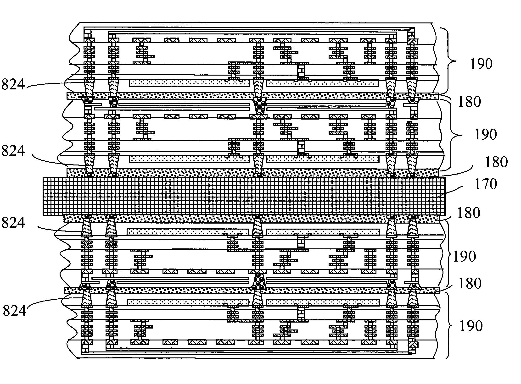
[0044] According to the present inventions, an integrated circuit device including a substrate, an interconnection level, a shielding level and a plurality of stitching studs is fabricated. The stitching studs pass through the substrate, extending to both surfaces of the substrate. In the invention, these stitching studs are formed by single trenches etched from the frontside surface or the backside surface, or by two mated trenches etched from both surfaces of the substrate. Then an insulating film is deposited in the trenches and the trenches are subsequently filled with a conductive material.

[0045] In the embodiments discussed below, two different types of application are present. The first exa...


PUM


Abstract

An integrated circuit device has a substrate, an interconnection level, a shielding level and a plurality of stitching studs. The substrate has a plurality of active devices, and the stitching studs pass through the substrate. The interconnection level is on the substrate, having a plurality of metal lines to provide interconnections between the active devices with a plurality of plugs. The shielding level is on the interconnection level, having an electromagnetic shielding pattern. The electromagnetic shielding pattern, the plugs, and the stitching studs are connected to form an electromagnetic shielding housing of the integrated circuit device.

Description

BACKGROUND [0001] 1. Field of Invention [0002] This invention relates to an integrated circuit structure and a manufacturing method thereof, and more particularly to the integration of an electromagnetic shielding and interconnect structures of a substrate. [0003] 2. Description of Related Art [0004] With the advances of microelectronic manufacturing technology and integrated circuit assembly techniques, a printed circuit board substrate usually comprises a plurality of metal layers, and interconnections therebetween to connect each two or more different metal layers. The multi-layer substrate provides a platform for mounting and interconnecting microelectronics devices and passive electronic devices, such as resistors, capacitors, and inductors. These passive electronic devices perform some pre-designed electronic functions required in electronic systems, such as personal computers, mobile phones, game consoles, personal digital assistants (PDAs), and television sets. [0005] Higher...

Claims


Application Information

Patent Timeline
IPC IPC(8): H01L21/3205H01L23/52H01L21/4763H01L21/60H01L21/768H01L23/48H01L23/522H01L23/538H01L23/552H01L25/065
CPCH01L21/76898H01L23/481H01L23/5225H01L23/5389H01L23/552H01L24/83H01L25/0652H01L2224/32145H01L2224/32225H01L2224/48091H01L2224/48145H01L2224/48227H01L2224/48235H01L2224/73265H01L2224/838H01L2924/01013H01L2924/01029H01L2924/01047H01L2924/01074H01L2924/01075H01L2924/01079H01L2924/01082H01L2924/04941H01L2924/0781H01L2924/10329H01L2924/14H01L2924/15311H01L2924/19041H01L2924/19042H01L2924/19043H01L2924/3025H01L24/32H01L24/48H01L2224/2919H01L2924/01006H01L2924/01033H01L2924/0105H01L2924/014H01L2924/0665H01L2924/0132H01L2924/10253H01L2924/13091H01L2924/00014H01L2924/00H01L2924/00015H01L2924/01031H01L2924/12042H01L2924/181H01L2224/49109H01L24/49H01L2924/00012H01L2224/45099H01L2224/45015H01L2924/207
Inventor TSENG, SHIH-HSIEN
Owner TSENG SHIH HSIEN
Why Eureka
Try Eureka