

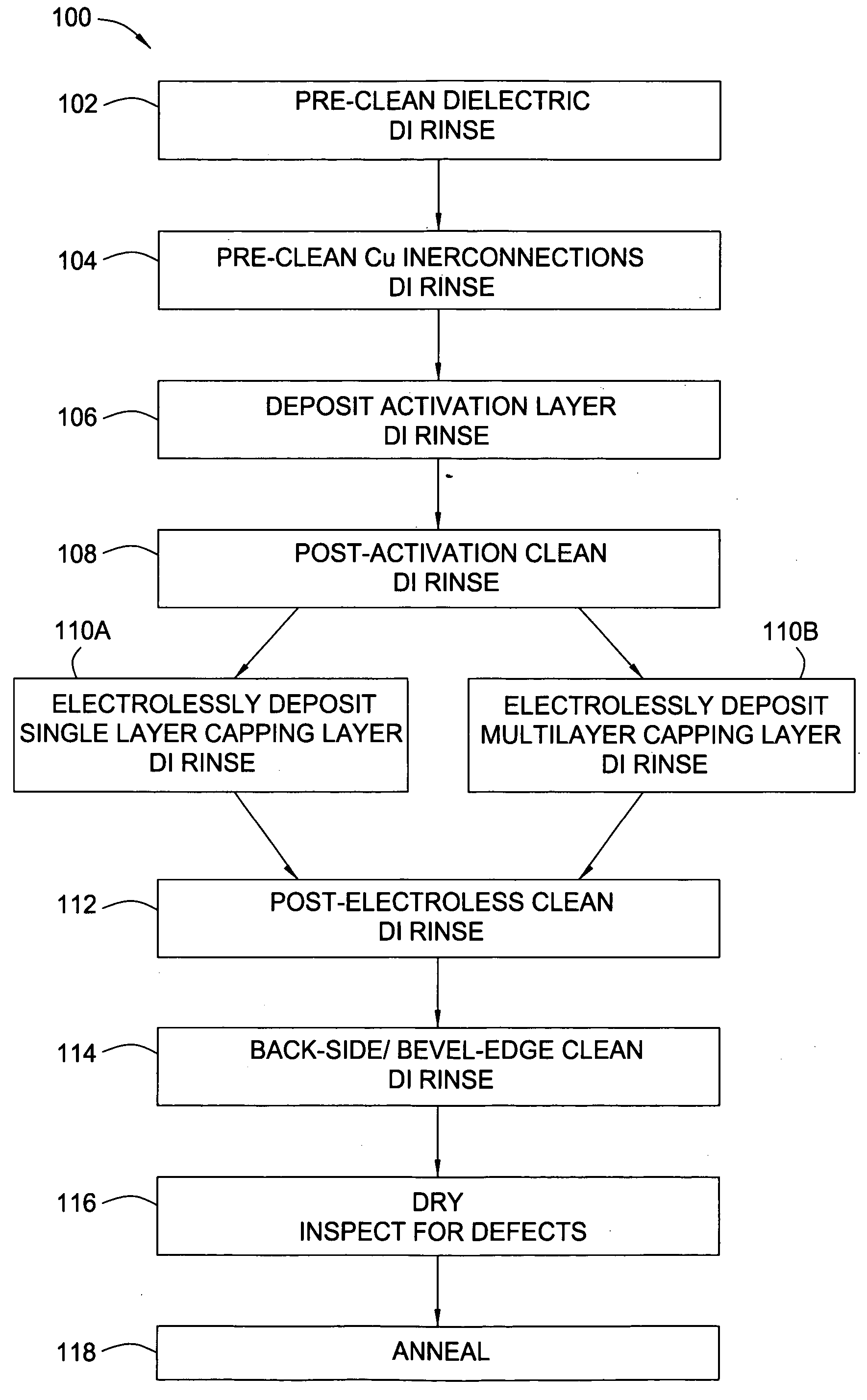
Method and tool of chemical doping CoW alloys with Re for increasing barrier properties of electroless capping layers for IC Cu interconnects
a technology of electroless capping layer and alloy, which is applied in the direction of liquid/solution decomposition chemical coating, coating, metallic material coating process, etc., can solve the problems of reducing the reliability of the overall circuit, reducing the resistance-capacitance delay constant of metal/dielectric system, and increasing the vulnerability of cu interconnect to diffusion and electromigration failure, etc., to achieve enhanced barrier resistance, enhanced barrier resistance to both copper
- Summary
- Abstract
- Description
- Claims
- Application Information
AI Technical Summary
Benefits of technology
Problems solved by technology
Method used
Image

Examples
Embodiment Construction
[0020] The words and phrases used herein should be given their ordinary and customary meaning in the art to one skilled in the art unless otherwise further defined. Electroless deposition is broadly defined herein as deposition of a conductive material generally provided as charged ions in a bath over a catalytically active surface to deposit the conductive material by chemical reduction in the absence of an external electric current.
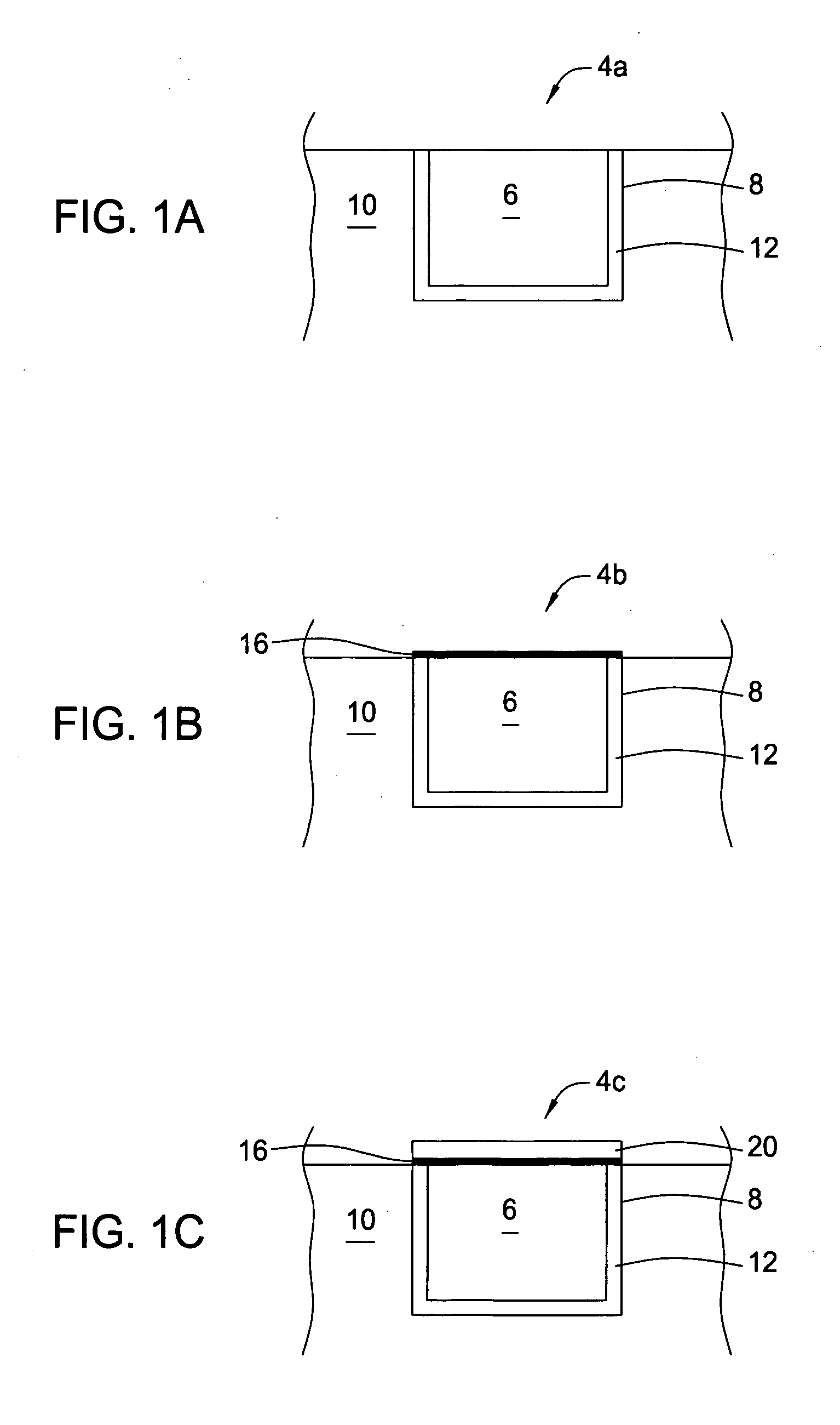
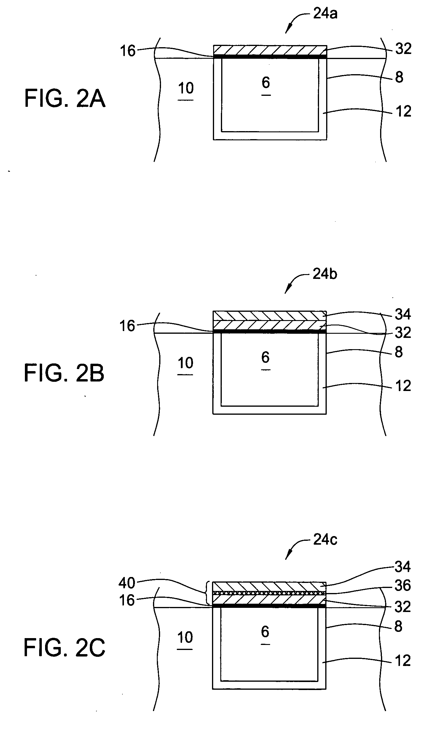
[0021]FIG. 1A shows a cross-sectional view of an interconnect 4a containing a conductive fill material 6 disposed within an interconnect opening 8 formed in a low-k dielectric material 10. Interconnect 4a, as well as other semiconductor features, are disposed on a substrate surface. Substrate surfaces on which embodiments of the invention may be useful include, but are not limited to, crystalline silicon (e.g., Si or Si), silicon oxide, silicon germanium, doped or undoped polysilicon, doped or undoped silicon, and silicon nitride. Other substrate surfa...
PUM
| Property | Measurement | Unit |
|---|---|---|
| concentration | aaaaa | aaaaa |
| concentration | aaaaa | aaaaa |
| temperature | aaaaa | aaaaa |
Abstract
Description
Claims
Application Information