Semiconductor light emitting diode and method for manufacturing the same

a technology of semiconductors and light-emitting diodes, which is applied in the direction of semiconductor devices, basic electric elements, electrical appliances, etc., can solve the problems of many limitations in the manufacturing process, increase in the number of inferior chips, and limited chip productivity per wafer

Inactive Publication Date: 2005-05-19
ITSWELL
View PDF3 Cites 133 Cited by
  • Summary
  • Abstract
  • Description
  • Claims
  • Application Information

AI Technical Summary

Benefits of technology

[0010] It is another object of the present invention to provide a simplified process of manufacturing a light emitting diode having a vertical electrode structure.

Problems solved by technology

Accordingly, the chip productivity per wafer is limited.
Since the insulating material is used for the base substrate, it is difficult to discharge static electricity incoming from outside, resulting in an increase in the number of inferior chips.
Using insulating base substrate induces many limitations in the manufacturing process.
Due to the low thermal conductivity of Sapphire, heat which is produced during operation is not emitted well.
Bad heat emitting disturbs applying a large current for high output power.

Method used


Image

  • Semiconductor light emitting diode and method for manufacturing the same
  • Semiconductor light emitting diode and method for manufacturing the same
  • Semiconductor light emitting diode and method for manufacturing the same

Examples


second embodiment

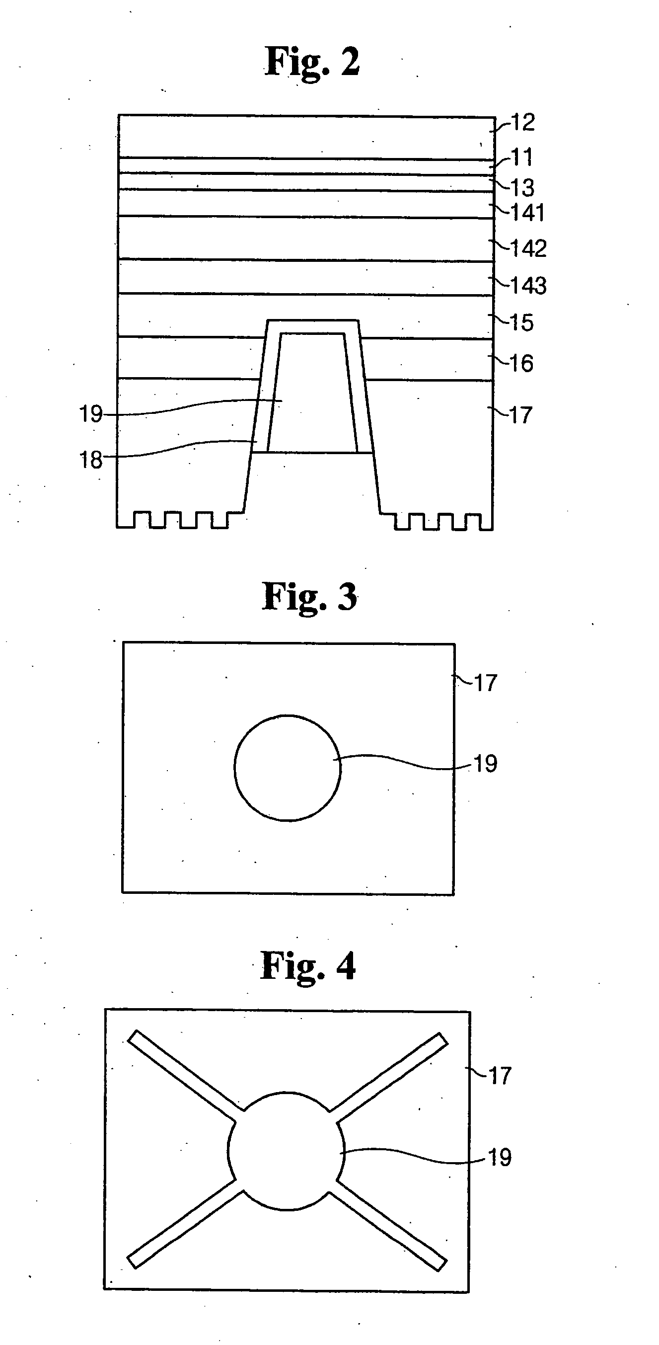
[0085]FIG. 4 is a top plan view illustrating the light emitting diode chip having a vertical electrode structure according to the present invention.

[0086] As shown in FIG. 4, the second electrode 19 is branched outside from the center circle so as to improve the current distribution and thermal emission in the second embodiment. The plan view of the second electrode 19 can be modified in various shapes.

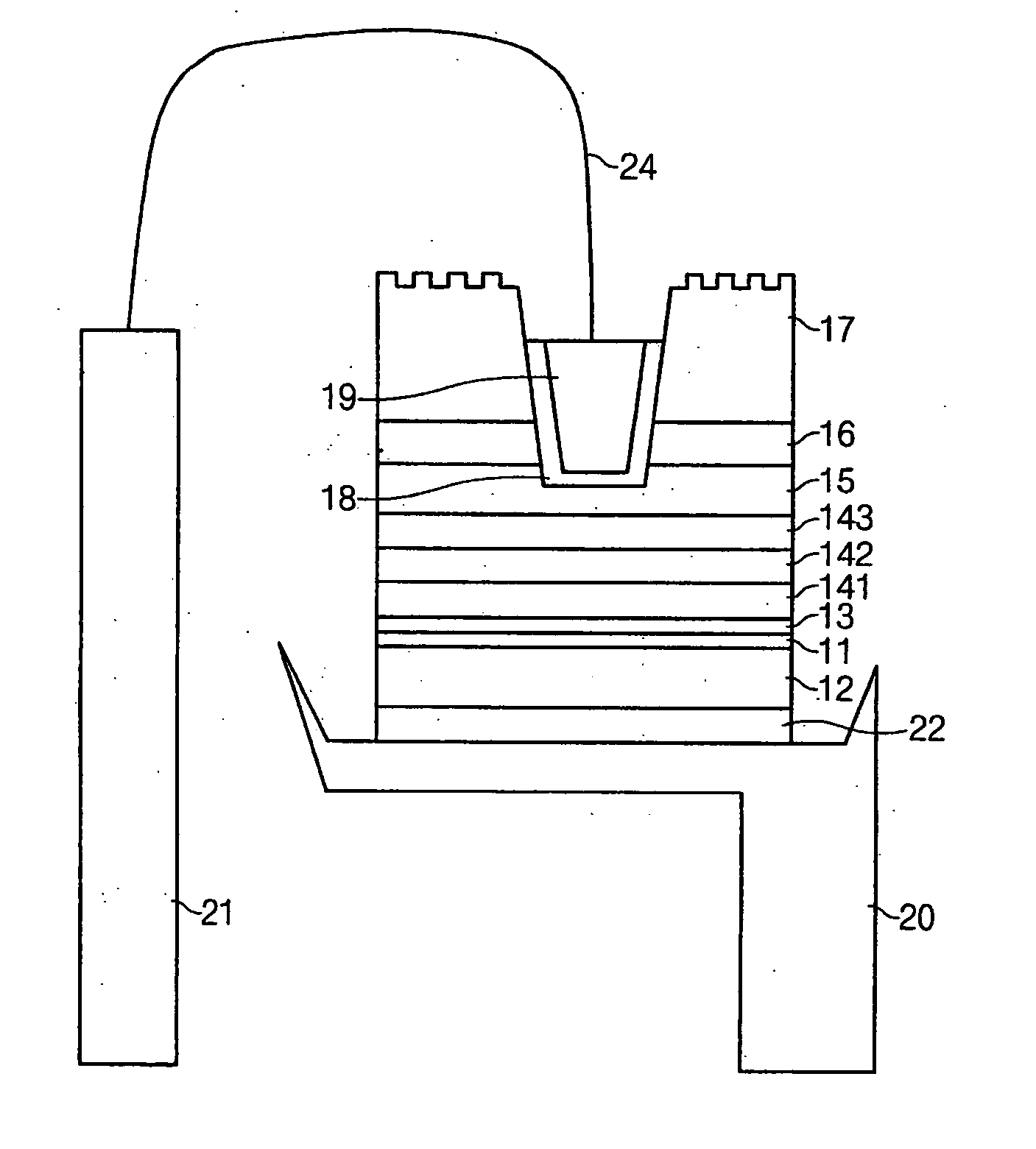
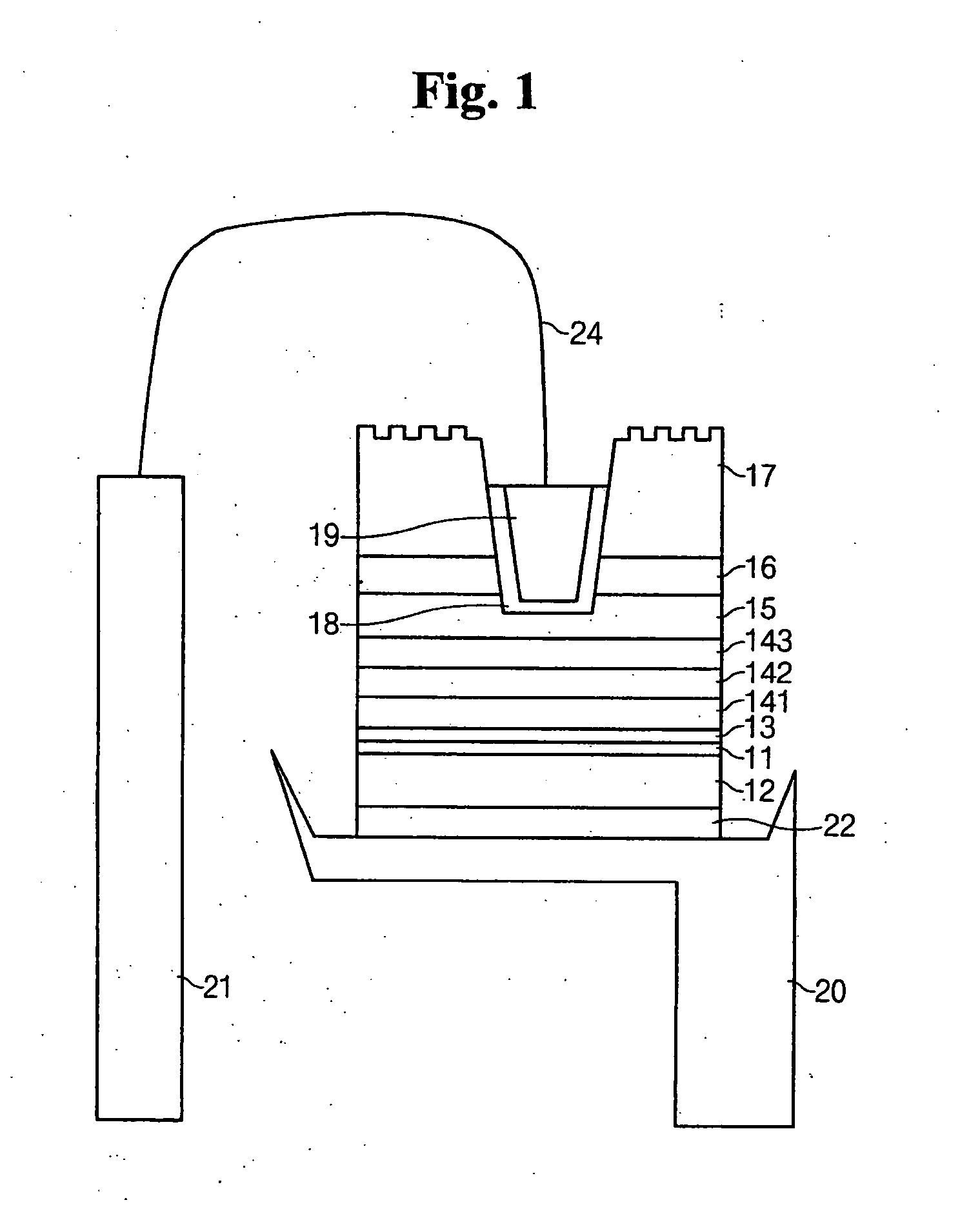
[0087] Now, a method of manufacturing a light emission diode having the above structure will be described.

[0088] The buffer layer 16, n-type contact layer 15, n-type clad layer 143, light emitting layer 142, p-type clad layer 141, and p-type contact layer 13 are deposited on the sapphire (Al2O3) substrate 17 in that order using any of metal organic chemical vapor deposition, liquid phase epitaxy, molecular beam epitaxy, hydride vapor phase epitaxy, metal organic vapor phase epitaxy (MOVPE), metal organic chemical vapor deposition, liquid phase epitaxy, molecular beam epitaxy, and va...

third embodiment

[0145] In the present invention, an electrode pad is formed on the sapphire substrate 17 by expanding the second ohmic layer 18 and the second electrode 19 outward the via hole in order to prevent the nitride series semiconductor layers 15, 141, 142, 143, and 11 from being damaged due to the pressure applied thereto when the second electrode 19 and the wire 24 are bonded. The shape and position of the second electrode 19 pad can be variously modified and it is possible to adopt the shape of FIG. 4.

[0146] In the meantime, the light is concentrated in the normal direction of the sapphire substrate 16 by the prominences and depressions on the surface of the sapphire substrate 17. Here, he unit length of prominence and depression are preferably greater than ¼n (“n” is refraction index. For the depression, “n” is the refraction index of sapphire and for the prominence, “n” is the refraction index of air) so as the prominence and depression to have photonic crystal characteristics.

fourth embodiment

[0147]FIG. 13 is a sectional view illustrating a light emitting diode chip having the vertical electrode structure according to the present invention, in which the light is extracted from the base substrate.

[0148] In the fourth embodiment, on behalf of the second ohmic layer, a transparent conductive substance such as ITO, ZrB, ZnO, InO, SnO, and the like is coated on the surface of sapphire substrate 17 and the second electrode 19 is narrowly formed only around the via hole. This is for broadening the light path by reducing the size of the opaque second electrode 19. In order to secure the space for bonding the wire, the ohmic layer 23 is coated on the surface of the sapphire substrate 17 at an area broader than a predetermined area.

[0149]FIG. 14 is a sectional view illustrating a light emitting diode having a vertical electrode structure according to a fifth embodiment of the present invention, FIG. 15 is a sectional view illustrating a light emitting diode chip having the vertic...


PUM


Abstract

Provided is a light emitting diode including a base substrate having a via hole, a buffer layer having a via hole which is partially overlapped with the via hole of the base substrate, a first conductive contact layer formed on the buffer layer, a first clad layer formed on the second conductive contact layer, a light emitting layer formed on the first clad layer, a second clad layer formed on the light emitting layer, a second conductive contact layer formed on the second conductive clad layer, a first electrode formed on the second conductive contact layer, and a second electrode connected with the first conductive contact layer through the via hole.

Description

BACKGROUND OF THE INVENTION [0001] (a) Field of the Invention [0002] The present invention relates to a semiconductor light emitting diode and a method for manufacturing the same, using a sapphire substrate etching technique. [0003] (b) Description of the Related Art [0004] A light emitting diode is an optical device that emits light when a forward current passes through it. The early light emitting diodes had a p-n junction structure of semiconductors and used compounds such as indium phosphorus (InP), gallium arsenic (GaAs), gallium phosphorus (GaP), etc. to emit red or green light. Since then, various kinds of light emitting diodes emitting blue or ultraviolet light have been developed to be used for the purposes of displays, light source devices, and environmental application devices. Recently, a white light emitting diode generating white light using three chips of red, green, and blue or phosphors has been developed, and is widely utilized for illumination field applications. ...

Claims


Application Information

Patent Timeline
Patent Type & Authority Applications(United States)
IPC IPC(8): H01L33/10H01L33/12H01L33/22H01L33/32H01L33/38H01L33/44H01L33/62
CPCH01L33/0079H01L33/20H01L33/382H01L33/405H01L2924/01322H01L2224/48091H01L2224/48247H01L2224/73265H01L2224/32245H01L2924/00014H01L2924/00H01L24/73H01L2224/32257H01L2224/8592H01L2924/10158H01L2924/12032H01L2924/181H01L33/0093H01L2924/00012
Inventor KIM, SEONG-JINCHOI, YONG-SEOKKIM, CHANG-YENHAN, YOUNG-HEONYU, SOON-JAE
Owner ITSWELL
Why Eureka
Try Eureka