Organic electroluminescent devices having a stability-enhancing layer

a technology of stability-enhancing layer and electroluminescent device, which is applied in the direction of discharge tube/lamp details, discharge tube luminescnet screen, other domestic articles, etc., can solve the problems of diffusive report and luminescence quenching in oleds, and achieve the effect of improving operational stability

Active Publication Date: 2005-05-19
GLOBAL OLED TECH
View PDF13 Cites 54 Cited by
  • Summary
  • Abstract
  • Description
  • Claims
  • Application Information

AI Technical Summary

Benefits of technology

[0006] Although it is believed that some organic layers doped with inorganic materials could cause EL quenching and operational stability deterioration in OLEDs, we unexpectedly found that stability enhancing layers, which include at least one organic host material and one inorganic dopant material and is in contact with the LEL can actually improve operational stability.

Problems solved by technology

However, Li and other metals are reported as being diffusive in organic layer resulting in luminescence quenching in OLEDs, for example, as reported by Haskal et al. in “Lithium-Aluminum Contacts for Organic Light-Emitting Devices”, Applied Physics Letters, 71, 1151 (1997).

Method used


Image

  • Organic electroluminescent devices having a stability-enhancing layer
  • Organic electroluminescent devices having a stability-enhancing layer
  • Organic electroluminescent devices having a stability-enhancing layer

Examples


example 1

Comparative Example

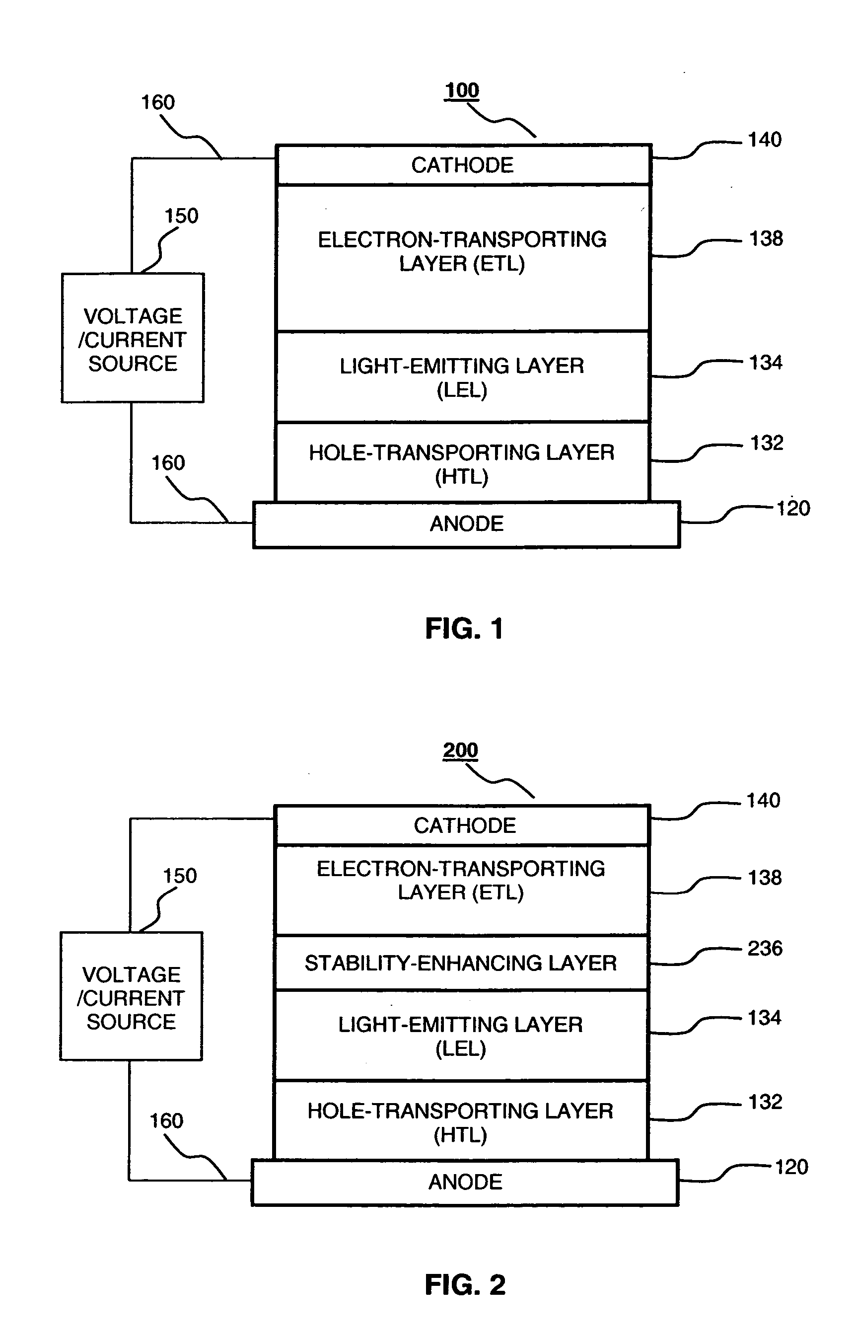
[0118] The preparation of a conventional OLED is as follows: A ˜1.1 mm thick glass substrate coated with a transparent ITO conductive layer was cleaned and dried using a commercial glass scrubber tool. The thickness of ITO is about 42 nm and the sheet resistance of the ITO is about 68 Ω / square. The ITO surface was subsequently treated with oxidative plasma to condition the surface as an anode. A layer of CFx, 1 nm thick, was deposited on the clean ITO surface as the HIL by decomposing CHF3 gas in an RF plasma treatment chamber. The substrate was then transferred into a vacuum deposition chamber (TROVATO MFG. INC) for deposition of all other layers on top of the substrate. All organic materials were sublimed before use. The following layers were deposited in the following sequence by evaporation from a heated boat under a vacuum of approximately 10−6 Torr: [0119] (1) a HTL, 90 nm thick, consisting of NPB; [0120] (2) a LEL, 20 nm thick, consisting of TBADN doped wi...

example 2

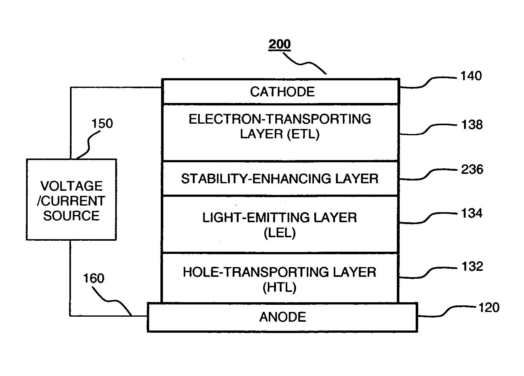
[0124] An OLED was constructed in the manner described in Example 1, except that one more layer was added onto the LEL. The layers were deposited in the following sequence: [0125] (1) a HTL, 90 nm thick, consisting of NPB; [0126] (2) a LEL, 20 nm thick, consisting of TBADN doped with 1.5% TBP by volume; [0127] (3) a stability-enhancing layer, 2.5 nm thick, consisting of Alq doped with 1.2% Li by volume; [0128] (4) an ETL, 32.5 nm thick, consisting of Alq; and [0129] (5) a cathode, approximately 210 nm thick, consisting of MgAg.

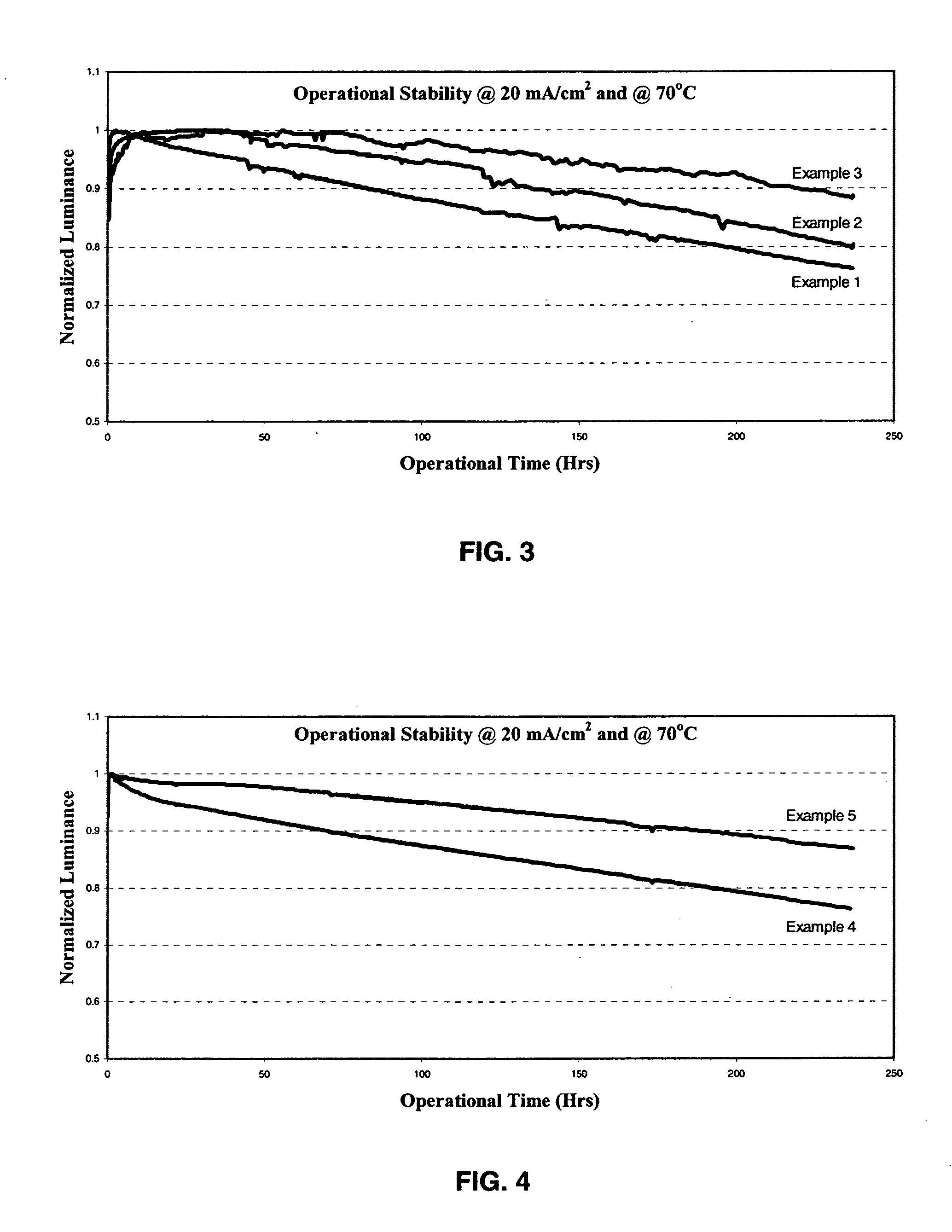
[0130] The completed device structure is denoted as ITO / CFx / NPB(90) / TBADN:TBP(1.5%)(20) / Alq:Li(1.2%)(2.5) / Alq(32.5) / MgAg. The EL performance of the device, measured at a current density of 20 mA / cm2, is shown in Table I, wherein the drive voltage, luminance, luminous efficiency, power efficiency, color coordinates CIEx,y, and the T90(70° C.) are listed. The normalized luminance vs. operational time is shown in FIG. 3.

example 3

[0131] An OLED was constructed in the manner described in Example 2, except in Step (3) wherein the thickness of the stability-enhancing layer is now increased to 15 nm, and except in Step (4) wherein the thickness of the ETL is now reduced to 20 nm. The completed device structure is denoted as ITO / CFx / NPB(90) / TBADN:TBP(1.5%)(20) / Alq:Li(1.2%)( 1 5) / Alq(20) / MgAg. The EL performance of the device, measured at a current density of 20 mA / cm2, is shown in Table I, wherein the drive voltage, luminance, luminous efficiency, power efficiency, color coordinates CIEx,y, and the T90(70° C.) are listed. The normalized luminance vs. operational time is shown in FIG. 3.

TABLE IExample(Type)LuminousPower(EL measuredVoltageLuminanceEfficiencyEfficiencyT90(70° C.)@ 20 mA / cm2)(V)(cd / m2)(cd / A)(lm / W)CIEyCIEy(Hrs)1 (Comparative)8.494222.110.780.1420.213842 (Inventive)9.043901.950.680.1340.1941353 (Inventive)8.323741.870.710.1340.202218

[0132] From the data shown in both Table I and FIG. 3, we find that ...


PUM


Abstract

An organic light-emitting device with enhanced operational stability comprising an anode; a hole-transporting layer disposed over the anode; a light-emitting layer disposed over the hole-transporting layer for producing light in response to hole-electron recombination, wherein the light-emitting layer includes at least one organic host material and one organic luminescent dopant material; a stability-enhancing layer disposed in contact with the light-emitting layer, wherein the stability-enhancing layer includes at least one organic host material and one inorganic dopant material; an electron-transporting layer disposed over the stability-enhancing layer; and a cathode disposed over the electron-transporting layer.

Description

FIELD OF INVENTION [0001] The present invention relates to improving the performance of an organic electroluminescent (EL) device. More specifically, this invention relates to improving the operational stability of an EL device. BACKGROUND OF THE INVENTION [0002] Organic electroluminescent (EL) devices (also known as organic light-emitting devices, organic light-emitting diodes, or OLEDs) are electronic devices that emit light in response to an applied potential. The structure of an OLED comprises, in sequence, an anode, an organic EL medium, and a cathode. The organic EL medium disposed between the anode and the cathode is commonly comprised of an organic hole-transporting layer (HTL) and an organic electron-transporting layer (ETL). Holes and electrons recombine and emit light in the ETL near the interface of HTL / ETL. Tang et al. demonstrated highly efficient OLEDs using such a layer structure in “Organic Electroluminescent Diodes”, Applied Physics Letters, 51, 913 (1987) and in c...

Claims


Application Information

Patent Timeline
Patent Type & Authority Applications(United States)
IPC IPC(8): H01L51/50
CPCH01L51/5048Y10S428/917H01L51/5052H10K50/165H10K50/14
Inventor LIAO, LIANG-SHENGKLUBEK, KEVIN P.
Owner GLOBAL OLED TECH
Why Eureka
Try Eureka