Crack and residue free conformal deposited silicon oxide with predictable and uniform etching characteristics

a conformal deposited silicon oxide and conformal etching technology, applied in the field of forming and/or etching silicon oxide during, can solve the problems of difficulty in cost effective integration of mems, additional processing required to integrate high-performance integrated circuitry, and affecting the etching effect of silicon oxide, etc., to achieve poor coverage of the underlying surface(s)

Active Publication Date: 2005-05-19
ROBERT BOSCH GMBH
View PDF19 Cites 45 Cited by
  • Summary
  • Abstract
  • Description
  • Claims
  • Application Information

AI Technical Summary

Benefits of technology

[0019] Iterative deposition and annealing of the silicon oxide layer in accordance with this aspect of the present invention results in a highly conformal silicon oxide layer having well-controlled stress and reduced contaminants and inclusions. The marked reduction in contaminants and inclusions allows the silicon oxide to be subsequently etched without formation of significant residue.
[0022] In a related aspect, an oxide layer provided by the method of the present invention may be deposited with well-defined and well-controlled stress. For example, it is often advantageous for an oxide layer to be formed over a MEMS component with slightly compressive stress such that a subsequent annealing step yields an oxide layer only slightly tensile, and thus unlikely to fail.
[0024] Further, the present invention provides a method of HF vapor etching an oxide layer formed in accordance with the present invention. This method effectively removes the oxide and any resulting etch residue where overly silicon-rich or carbon contaminated conditions exist.

Problems solved by technology

However, it can be difficult to cost effectively integrate MEMS that employ a hermetically sealed metal container or a bonded semiconductor or glass-like substrate to protect the mechanical structures on the same substrate with high performance integrated circuitry.
In this regard, the additional processing required to integrate the high performance integrated circuitry tends to either damage or destroy the mechanical structures.
Further, such oxides are often formed or deposited in a manner that provides poor coverage of the underlying surface(s).
Moreover, the removal of conventional oxides during the formation of MEMS may produce an etch residue on the mechanical structures during the encapsulation process.
In practice, MEMS formed in accordance with conventional techniques often suffer from significant process-induced performance variations or outright component failure.
To a great extent, inadequacies associated with the formation and / or removal of oxide layers account for many of these failures and undesired performance variations.
First, many conventional oxide layers crack during MEMS fabrication, and / or damage or crack the MEMS structure on which they are deposited.
Both highly tensile and highly compressive oxide layers are undesirable.
Highly tensile oxide layers may deform delicate MEMS components or crack outright.
Highly compressive oxide layers may also deform MEMS components or cause tensile cracking in these components or in adjacent materials.
Under the combined effect of these tendencies, an oxide layer deposited at moderate temperature may crack or may damage the MEMS structures when subsequently heated to significantly higher temperatures.
Unfortunately, highly conformal, conventional oxides are often susceptible to cracking and often contain materials that result in residue formation when the oxide is subsequently etched.
Such contaminates promote the development of etch residues.
Etch residues, which tend to be silicon in nature, can accumulate to the point where the etching process becomes uneven across an etch surface or impossible.
Etch residues can accumulate to the point where device functionality becomes impaired.
Unlike many conventional semiconductor fabrications, a wet etching process often cannot be applied to removal of an accumulated residue during some MEMS fabrications.
Unfortunately, many of these desirable properties are at odds one with another.
For example, highly conformal, conventional oxides are prone to cracking and often contain contaminants that promote etch residue.

Method used


Image

  • Crack and residue free conformal deposited silicon oxide with predictable and uniform etching characteristics
  • Crack and residue free conformal deposited silicon oxide with predictable and uniform etching characteristics
  • Crack and residue free conformal deposited silicon oxide with predictable and uniform etching characteristics

Examples


Embodiment Construction

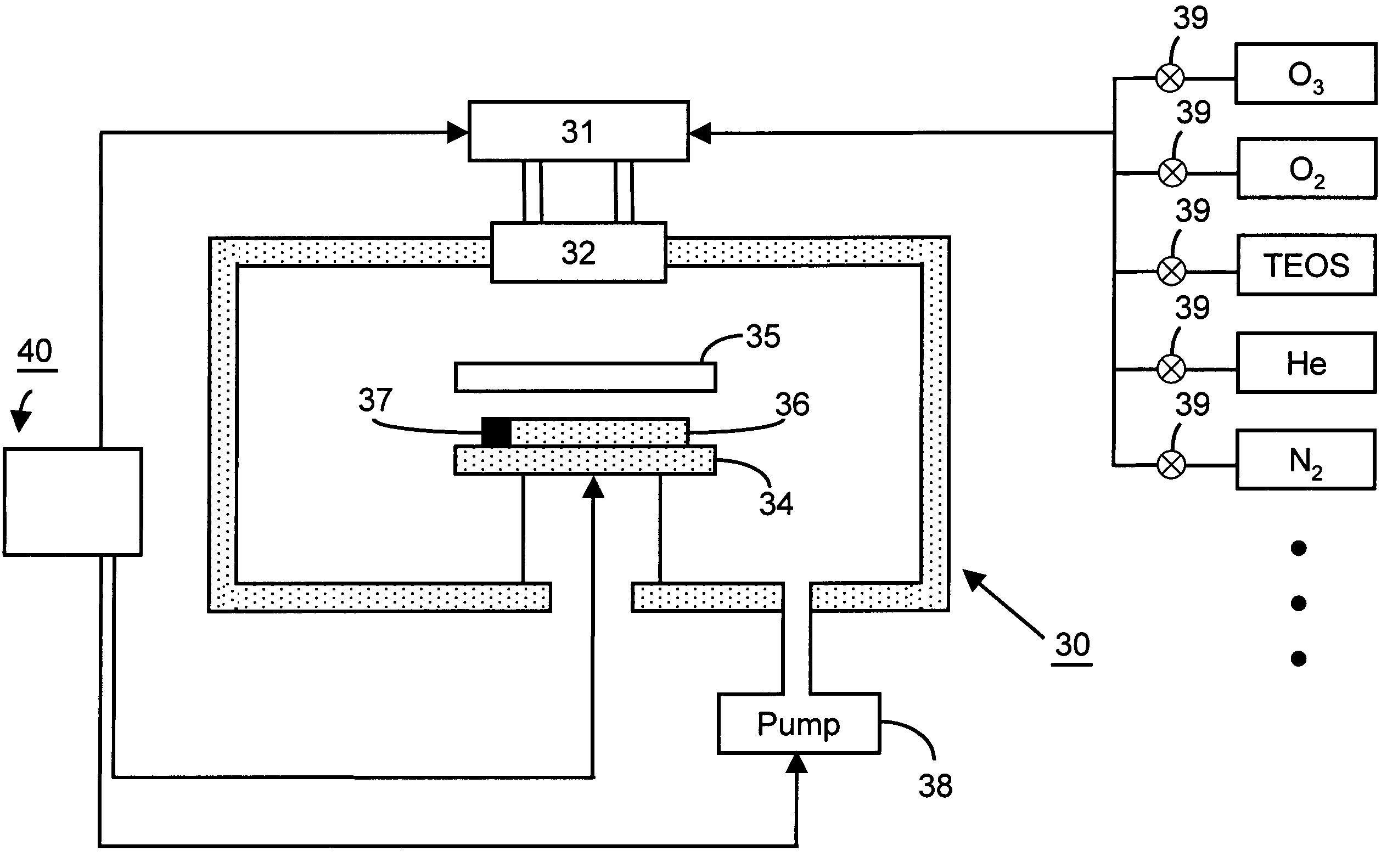
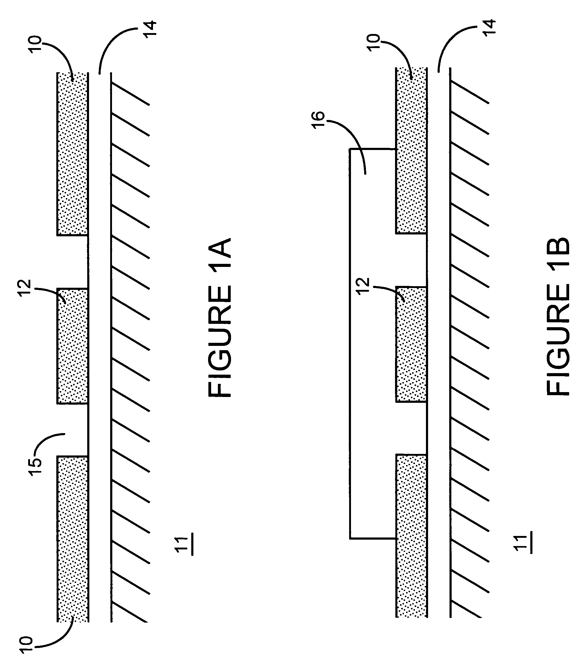
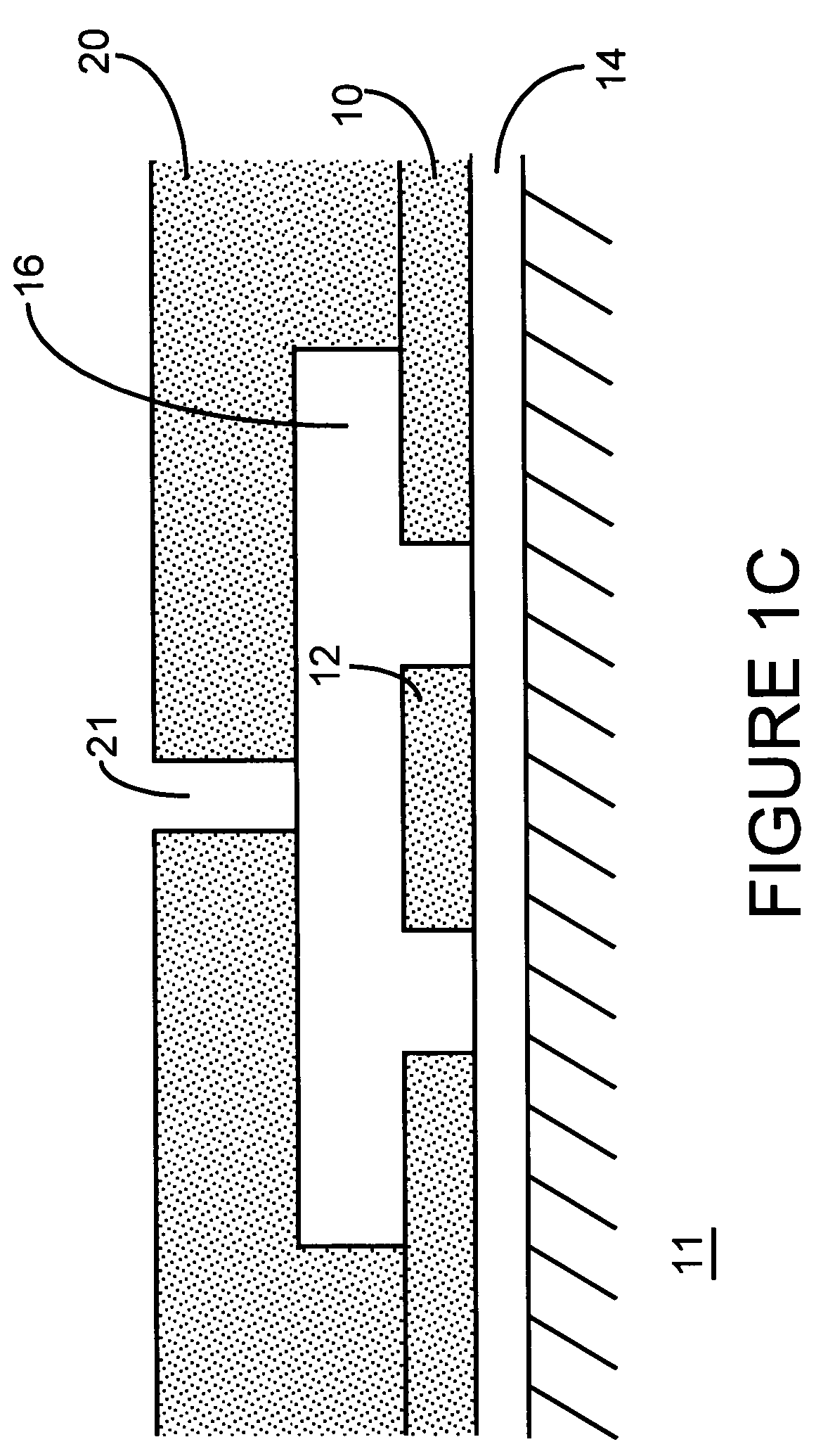
[0034] The present invention, in its multiple related aspects, is described below using a number of examples. For clarity, these examples are drawn to some specific teaching embodiments.

[0035] In a first aspect, the present invention recognizes a unique combination of benefits afforded by the iterative annealing of an oxide layer under prescribed conditions. The term “layer” is used as a practical description for any spatially and / or temporally specific oxide formation. It should not be read as being limited to only long horizontally disposed structures, although such structures are most commonly formed by conventional deposition techniques. Any area portion, segment, spot, strata, etc., may be considered a “layer” for purposes of this description.

[0036] By “iterative”, i.e., one or more times following oxide layer formation, annealing an oxide layer according to the dictates of the present invention, the stress of the oxide is well-controlled and contaminates and inclusions withi...


PUM

PropertyMeasurementUnit
temperatureaaaaaaaaaa
thicknessaaaaaaaaaa

Abstract

A silicon oxide layer is formed by oxidation or decomposition of a silicon precursor gas in an oxygen-rich environment followed by annealing. The silicon oxide layer may be formed with slightly compressive stress to yield, following annealing, an oxide layer having very low stress. The silicon oxide layer thus formed is readily etched without resulting residue using HF-vapor.

Description

BACKGROUND [0001] The present invention relates generally to a method of forming and / or etching silicon oxide during the fabrication of a semiconductor structure, an optical device, or an electromechanical system. Silicon oxide layers formed in accordance with the present invention have particular application in the field of microelectromechanical systems (MEMS). [0002] The term “MEMS” is used to describe a broad class of electromechanical systems having one or more micro and / or nano-sized components. MEMS are characterized in their implementation by the use of micro-machining techniques, such as lithographic and other precision fabrication techniques, to reduce mechanical components to a scale generally comparable to microelectronics. MEMS are further characterized in most instances by the operative assembly, arrangement and / or formation of these miniaturized components on a silicon substrate. Contemporary examples of MEMS-implemented devices include sensors, actuators, gyroscopes,...

Claims


Application Information

Patent Timeline
Patent Type & Authority Applications(United States)
IPC IPC(8): B05D5/12C23C16/00C23C16/04C23C16/40C23C16/56H01L21/316
CPCC23C16/045C23C16/402C23C16/56H01L21/31612H01L21/0228H01L21/02337H01L21/02164
Inventor PARTRIDGE, AARONLUTZ, MARKUSKRONMUELLER, SILVIA
Owner ROBERT BOSCH GMBH
Why Eureka
Try Eureka