Lithographic interferometer system

a technology of interferometer and lithography, which is applied in the direction of electrical equipment, instruments, basic electric elements, etc., can solve the problems of limiting the flexibility and affecting the accuracy of the combined system

Active Publication Date: 2005-05-26
ASML NETHERLANDS BV
View PDF11 Cites 38 Cited by
  • Summary
  • Abstract
  • Description
  • Claims
  • Application Information

AI Technical Summary

Benefits of technology

[0026] The second type, the differential plane mirror interferometer, uses a measurement set-up in which a measuring beam is again reflected by a mirror fixed to the object, and where a “reference beam” is reflected by at least one mirror not fixed to the beam-splitter. Various possible configurations exist to reflect the reference beam. For example, the reference beam may be reflected b...

Problems solved by technology

The overlap may cause constructive or destructive interference, depending on the phase difference of the radiation in the two bundles.
A disadvantage of the combination interferometer system is the complexity of the overall system, requiring t...

Method used


Image

  • Lithographic interferometer system
  • Lithographic interferometer system
  • Lithographic interferometer system

Examples


Embodiment Construction

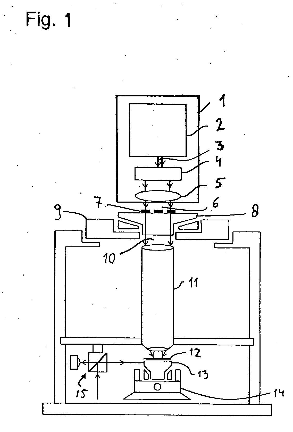
[0073]FIG. 1 schematically depicts a lithographic apparatus according to an embodiment of the invention. The arrangement of the depicted lithographic system is in principle well known in the art. A brief description will therefore suffice for a person skilled in the art.

[0074] Herein, 1 indicates an illumination system, comprising a source 2 of radiation, emitting a beam 3 of radiation. A beam expander 4 and beam shaping means 5 form the beam 3 into projection beam 6. Projection beam 6 passes through mask 7, which is placed on mask table 8, which is moveable by means of mask table moving means 9.

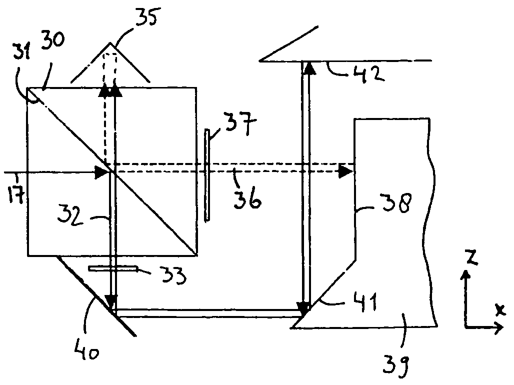
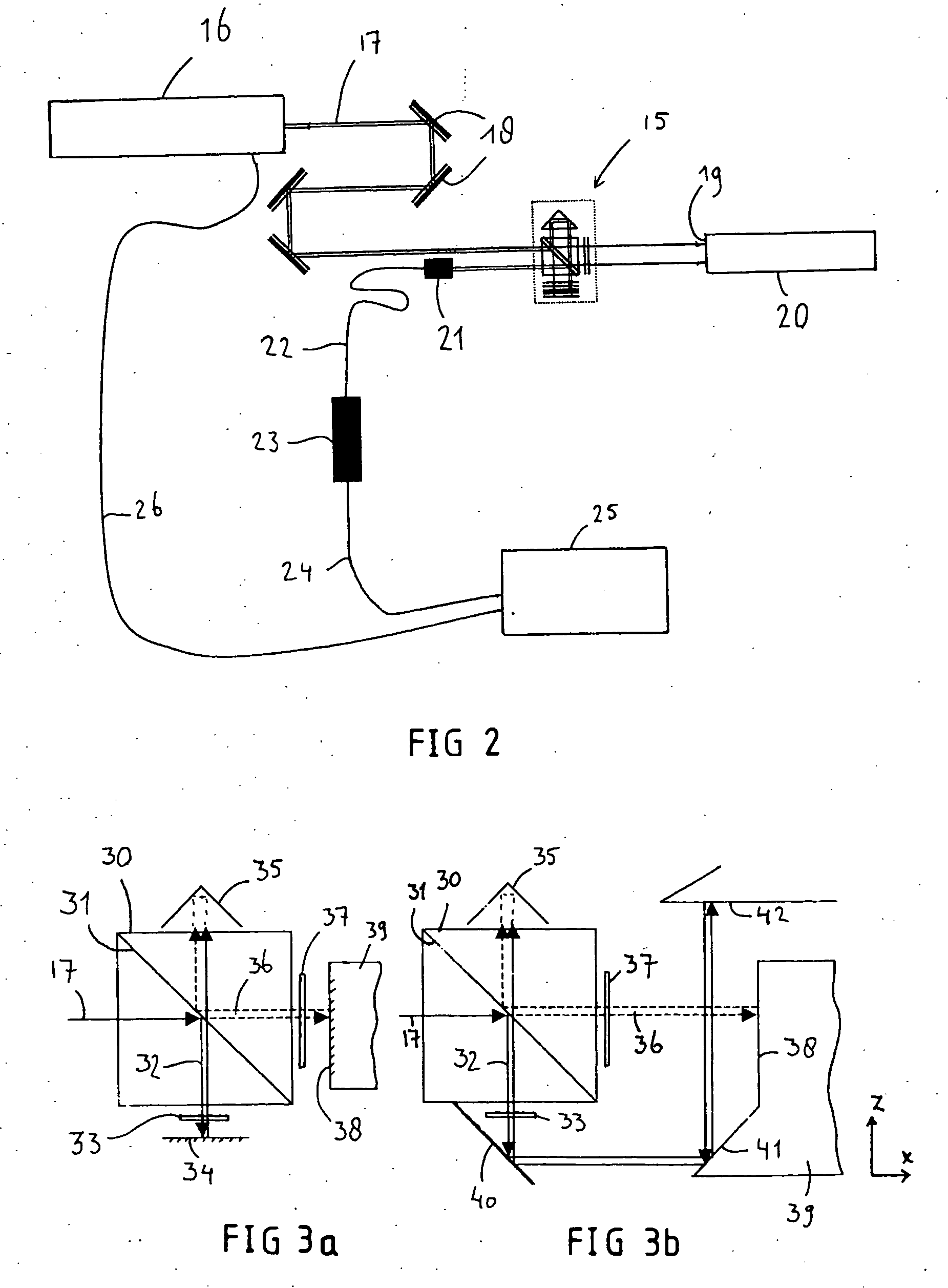
[0075] A beam 10 passes through projection optics 11 and strikes the surface of wafer 12, which is located on wafer stage 13. The wafer stage 13 may be displaced by means of wafer stage moving means 14, and the displacement maybe determined by means of (schematically) interferometer system 15.

[0076] The illumination system 1 comprises a source 2 of radiation, for example a laser, having a...


PUM


Abstract

An improved lithographic interferometer system, is presented herein. The lithographic interferometer system comprises a beam generating mechanism, mirrors which reflect those beams, and detection devices for detecting an interference pattern of overlapping reflected beams. The beam generating mechanism comprises a beam-splitter, which splits the beams into reference beams and measuring beams, a reference mirror that provides a plane mirror interferometer, and a reflective surface that emits at least one reference beam used in a differential plane mirror interferometer.

Description

BACKGROUND OF THE INVENTION [0001] 1. Field of the Invention [0002] The present invention relates to lithographic apparatus and, more particularly, to an improved interferometer system employed in a lithographic apparatus. [0003] 2. Description of the Related Art [0004] A lithographic apparatus is a machine that applies a desired pattern onto a target portion or target field of a substrate. Lithographic apparatus can be used, for example, in the manufacture of integrated circuits (ICs). In that circumstance, a patterning device, such as a mask (i.e., reticle), may be used to generate a circuit pattern corresponding to an individual layer of the IC, and this pattern can be imaged onto a target field (e.g. comprising part of one or several dies) on a substrate (e.g. a silicon wafer) that has a layer of radiation-sensitive material (resist). [0005] In general, a single substrate will contain a network of adjacent target portions or fields that are successively exposed. Known lithograph...

Claims


Application Information

Patent Timeline
IPC IPC(8): G01B9/02G01B11/00G03F7/20H01L21/027
CPCG03F7/70775G01B9/02019G01B2290/70G01B9/02027G01B9/02018G01B9/02021
Inventor EUSSEN, EMIEL JOZEF MELANIEBEEMS, MARCEL HENDRIKUS MARIAVAN DER PASCH, ENGELBERTUS ANTONLUS FRANSISCUS
Owner ASML NETHERLANDS BV
Why Eureka
Try Eureka