Photolithographic patterning process using a carbon hard mask layer of diamond-like hardness produced by a plasma-enhanced deposition process

a technology of diamond-like hardness and photolithography, which is applied in the direction of photomechanical treatment, instruments, electrical equipment, etc., can solve the problems of not being generally suitable, open, and not being able to control the polymer formed from the resist during the etching process, and achieve the effect of enhancing the etching process and optimal diamond-like hardness properties

Inactive Publication Date: 2005-05-26
CHANGXIN MEMORY TECH INC
View PDF17 Cites 45 Cited by
  • Summary
  • Abstract
  • Description
  • Claims
  • Application Information

AI Technical Summary

Benefits of technology

[0015] One advantage of the invention lies in depositing the carbon hard mask layer by means of a plasma enhanced deposition process and carrying out the deposition in such a manner that the carbon hard mask layer, in at least one layer thickness section, has a hardness comparable to that of diamond.
[0016] In this context, it is possible to provide for the layer thickness section to extend over the entire carbon hard mask layer and therefore for the carbon hard mask layer to have optimum diamond-like hardness properties and etching resistance properties over its entire thickness. However, it is also possible for the layer to have a diamond-like hardness in only a limited layer thickness section and to have a different hardness in the remaining layer thickness sections.
[0017] Where the following text makes frequent mention of the term “diamond-like” or “graphite-like”, these terms do not necessarily relate to the structure of the layer applied. Even if the layer is applied with a diamond-like hardness, the crystal structure may and generally will be an amorphous carbon structure.
[0018] During the production of the diamond-like layer thickness section, the parameters used for the deposition can be set in such a manner that graphite-like regions which are formed are removed again in situ by means of subsequent etching processes, and that diamond-like regions which are formed are retained. Parameters of this nature which enhance the etching processes include, for example, the supply of ionizable gases, such as argon and / or neon, into the reactor chamber, which brings about additional ion bombardment during the deposition. A further parameter which promotes the etching processes is the hydrogen content in the gas phase.
[0019] These parameters can be varied during the layer growth, so that the properties of the carbon hard mask layer formed can be varied over its layer thickness.
[0020] The patterning process can be carried out such that a carbon hard mask layer as indicated is applied to the substrate to be patterned, and then a photoresist layer is applied to the carbon hard mask layer. After the exposure and developing of the photoresist layer in order to produce a predetermined pattern, this pattern is transferred to the carbon hard mask layer. The carbon hard mask layer then serves as the actual etching mask for etching of the substrate.

Problems solved by technology

In particular during the etching of contact holes with a very high aspect ratio, photoresist masks of this type have the significant drawback that it is not possible to control the polymers formed from the resist during the etch.
The polysilicon hard mask layer is in this case deposited in a furnace process at temperatures of between 600° C. and 700° C., which can give rise to problems as a result of the thermal load imposed on the circuit structures which have already been produced.
One general problem of the hard mask materials which have just been referred to is that they have to be opened up in a dedicated etching step.
A further drawback is that they are not generally suitable—as in the example of polysilicon—for use as antireflection coatings.
However, these layers cannot be used as hard mask layers, and the reflection can only be reduced to approx.
Furthermore, inorganic oxynitrides which are applied using a CVD process are known for use as antireflection layers, but the reflection cannot be reduced to below 10%.
At least for use in oxide etching processes, these layers are likewise not suitable for use as hard mask layers.
However, if the deposition has to take place on a topographic pattern which has holes, trenches or elevations, the PECVD process has the drawback that the carbon layer cannot be optimally introduced into the trenches and holes and also does not have a planarizing action.
A further drawback is that in general the hard mask quality of the carbon hard mask layer increases with increasing hardness, i.e. an increasing diamond fraction, in the layer and with a decrease in hydrogen content, but the two criteria can only be realized to a limited extent using the PECVD process.
However, there is no more accurate description of how the process is to be managed to ensure that a carbon hard mask layer of high quality can be achieved.

Method used


Image

  • Photolithographic patterning process using a carbon hard mask layer of diamond-like hardness produced by a plasma-enhanced deposition process
  • Photolithographic patterning process using a carbon hard mask layer of diamond-like hardness produced by a plasma-enhanced deposition process
  • Photolithographic patterning process using a carbon hard mask layer of diamond-like hardness produced by a plasma-enhanced deposition process

Examples


Embodiment Construction

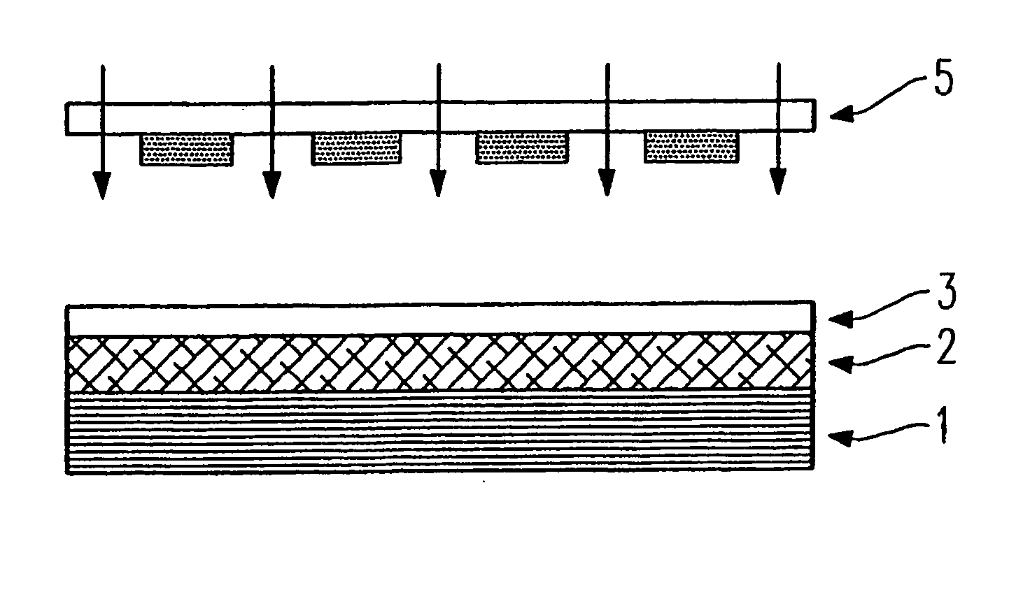
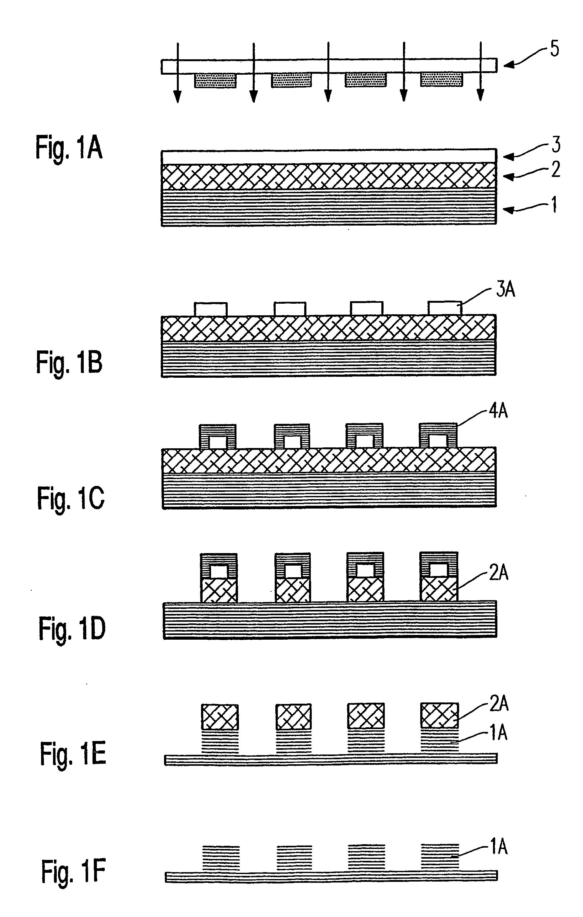
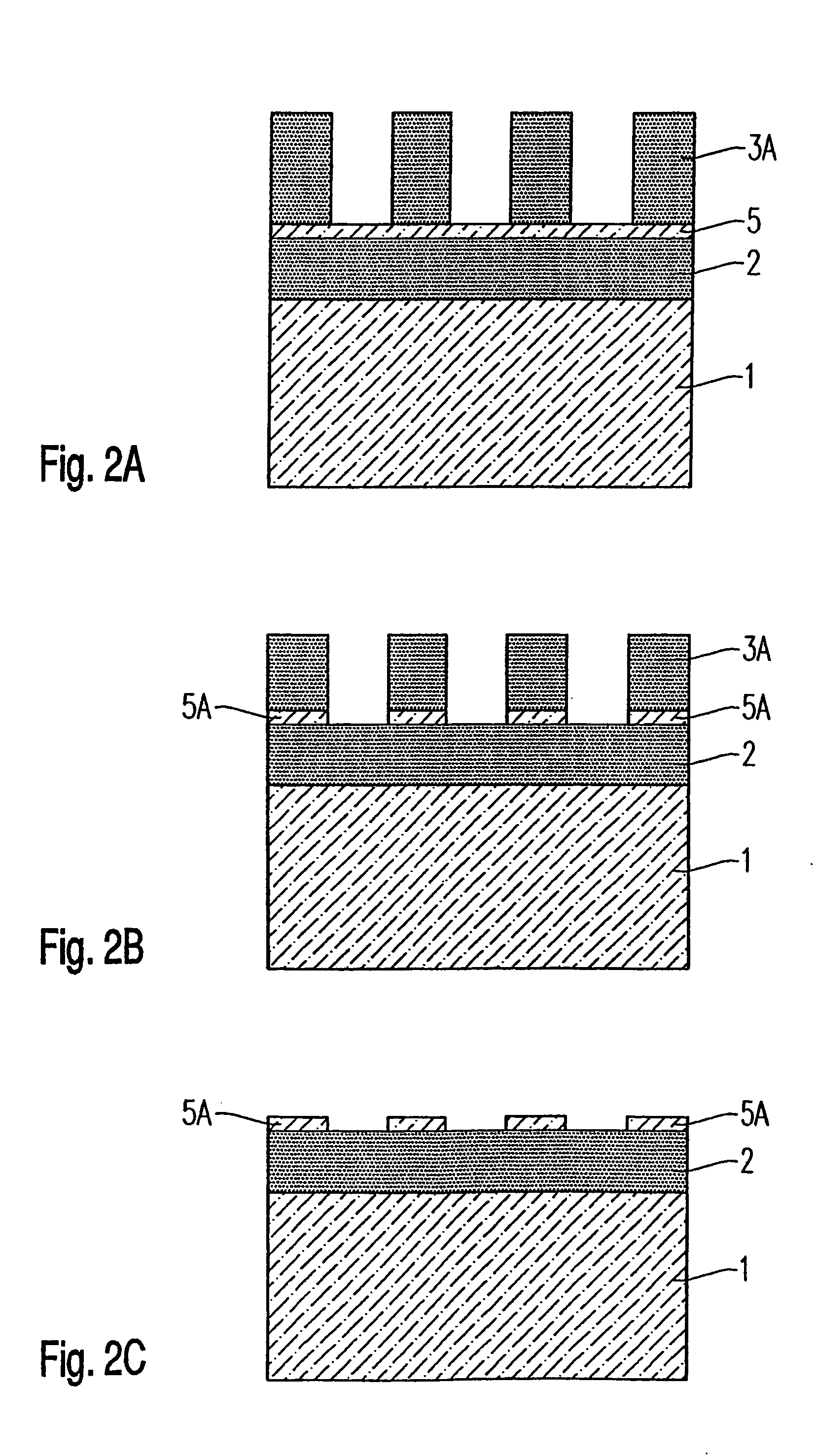
[0033] In accordance with FIG. 1A, a substrate 1 which is to be patterned is provided, which substrate may, for example, be a chip or wafer into which a matrix-like arrangement of trench capacitors has already been processed, these trench capacitors each belonging to memory cells. The patterning process illustrated in the following text by way of example is intended to produce insulation regions (STI) between the trench capacitors. Since the sections which are to be removed in order to produce the insulation regions also in each case include partial sections of the processed trench capacitors, accordingly it is also necessary to etch silicon oxide, since the trench capacitors generally have an insulation collar including silicon oxide.

[0034] A carbon hard mask layer 2 is applied to the substrate 1 which has undergone preliminary processing of this nature. As described, the production of the carbon hard mask layer 2 is effected by a plasma enhanced deposition process. In the specifi...


PUM

PropertyMeasurementUnit
temperatureaaaaaaaaaa
exposure wavelengthsaaaaaaaaaa

Abstract

A carbon hard mask layer is applied to a substrate to be patterned by means of a plasma-enhanced deposition process in such a manner that it has a hardness comparable to that of diamond in at least one layer thickness section. During the production of this diamond-like layer thickness section, the parameters used in the deposition are set in such a manner that growth regions which are produced in a form other than diamond-like are removed again in situ by means of subsequent etching processes and that diamond-like regions which are formed are retained.

Description

CLAIM FOR PRIORITY [0001] This application claims priority to International Application No. PCT / DE02 / 04034, which was published in the German language on May 8, 2003, which claims the benefit of priority to German Application No. 101 53 310.1, which was filed in the German language on Oct. 29, 2001. TECHNICAL FIELD OF THE INVENTION [0002] The present invention relates to the field of patterning processes for semiconductor technology, and in particular, in which a layer at the surface of a substrate is to be patterned. BACKGROUND OF THE INVENTION [0003] The production of semiconductor components often entails the requirement that in one process step patterning by etching must be carried out, in which the sections to be removed are formed at least in part by silicon oxide or silicon nitride. One example of this is the fabrication of semiconductor memory cells which have a trench capacitor and a select transistor. Whereas the trench capacitor on one side is electrically connected to th...

Claims


Application Information

Patent Timeline
Patent Type & Authority Applications(United States)
IPC IPC(8): G03F7/36H01L21/033H01L21/308H01L21/311H01L21/314
CPCH01L21/0332H01L21/3146H01L21/31144H01L21/3081H01L21/02274H01L21/02115H01L21/02205H01L21/0214G03F7/40H01L21/02107H01L21/0271
Inventor CZECH, GUNTERFUELBER, CARSTENKIRCHHOFF, MARCUSSTEGEMANN, MAIKVOGT, MIRKOWEGE, STEPHAN
Owner CHANGXIN MEMORY TECH INC
Why Eureka
Try Eureka