Wire bond integrity test system

a testing system and wire bond technology, applied in the field of semiconductor device assembly, can solve the problems of increased cycle time, reduced production rate, work stoppage, etc., and achieve the effect of minimizing errors

Inactive Publication Date: 2005-05-26
TEXAS INSTR INC
View PDF14 Cites 1 Cited by
  • Summary
  • Abstract
  • Description
  • Claims
  • Application Information

AI Technical Summary

Benefits of technology

[0010] It is an object of the current invention to provide an improved bond integrity detection system which minimizes errors at the first bond.

Problems solved by technology

Work stoppages, often signaled by a red light positioned atop the equipment, can occur if the machine is out of material, or if a failure in the bonding cycle is detected.
Excessive stoppage events require additional operators, increase cycle time, lower production rates, and generally contribute to an increase in the device cost, and a decrease in productivity.
Frequently work stoppages result from a reported failure of a “lifted ball bond”.
This failure is correctly detected by the bond integrity test system, as a failure.
However, the bonder BITS frequently reports an erroneous “lifted ball” signal, which in turn requires the attention of an operator to investigate the cause, define the correction, and restart the bonding cycle.
While bond integrity tests do generate a number of erroneous readings, it is necessary that high speed bonders include these automated tests, because failure to detect mis-bonds during the process, and halt the bonding, destroy a large number of chips and substrates if a correction were not made.
Without a detection mechanism, there could be a significant cost increase for additional operators and surveillance to minimize the number of devices erroneously bonded.
One common erroneous reading is a “false lifted ball”; a false indication that the ball bond to the chip pad is not properly connected.
However, very small changes will be detected, and a failure reported, whether real or false.
The fault is detected in the continuity signature, and a shift in the signature may cause a work stoppage.
Necessarily, bond integrity detection systems are very sensitive, which contributes to the fact that they do cause a number of false work stoppages.
Attempts to raise the voltage or current in the fine wire to generate a larger current flow so as to provide larger values for error detection often are harmful to the device under assembly, and therefore, is not an acceptable solution.

Method used


Image

  • Wire bond integrity test system
  • Wire bond integrity test system
  • Wire bond integrity test system

Examples


Embodiment Construction

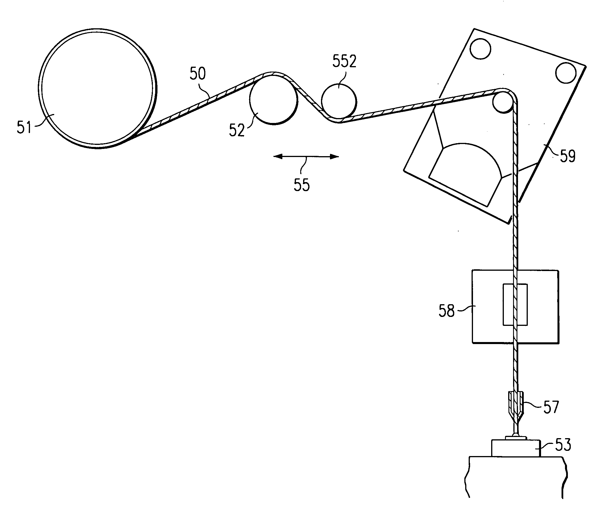
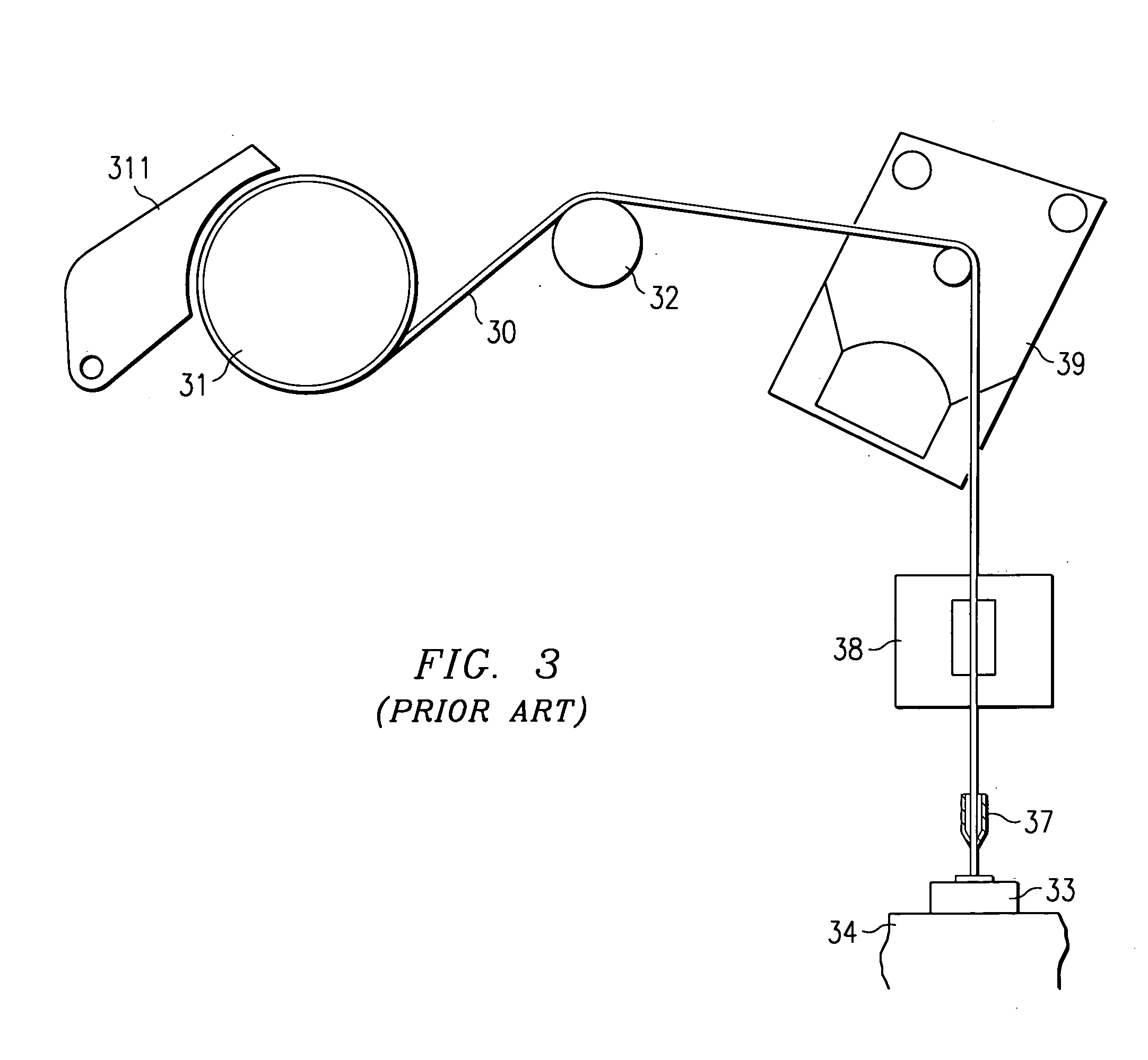
[0020]FIG. 3 schematically depicts the path followed by the bond wire on many existing wire bonders. A fine gold wire 30, twenty-five microns or less in diameter, is fed from a wire spool assembly 31 to a protruding contact and guide mechanism 32, commonly referred to as a diverter. Diverter 32 makes electrical and mechanical contact with the wire 30, and helps control tension on the wire. The spool assembly 31 includes a wire wound spool and a spring held cover 311 for contacting the wire as it is fed from the spool.

[0021] The path of the wire continues through an air guide 39, a complex wire clamp assembly 38, and an insulating ceramic capillary 37. A ball formed at the end of the capillary is brought into contact with the bond pad of a grounded semiconductor device 33, situated on the work station 34 of a bonder. A transducer is energized to produce current and force for a sufficient time to cause the formed ball to bond to the pad while the wire clamp is in the open state. Afte...


PUM

PropertyMeasurementUnit
diameteraaaaaaaaaa
diameteraaaaaaaaaa
diameteraaaaaaaaaa

Abstract

An improved bond integrity test system is provided by eliminating the spring loaded wire spool cover which contributes to particulate matter, and by addition of a second contact diverter in the wire path. These improvements have been shown to decrease false lifted ball bond reports by 68%, and therefore to improve productivity and accuracy of the test system. Such changes are readily adapted to current bonders, as well as to new designs.

Description

FIELD OF THE INVENTION [0001] This invention relates generally to the assembly of semiconductor devices, and more specifically to wire bonding equipment, and wire bond testing systems. BACKGROUND OF THE INVENTION [0002] Automated wire bonders are employed to make electrical connections between input / output (I / O) pads of semiconductor chips and conductive leads on substrates or lead frames. Most often, each connection is made by way of a very thin gold wire, fed from a spool, through a series of control mechanisms to a capillary where by a combination of heat and ultrasonic energy, a first or ball bond is attached to the chip pad, and a second or stitch bond to the substrate. State-of-the-art bonders operate at very high speeds. For example one interconnection every 250 milliseconds is not an unusual bonding rate. [0003] High-speed bonding equipment is typically programmed by a technician or operator for a selected device lot, the materials are supplied, and the equipment is then exp...

Claims


Application Information

Patent Timeline
Patent Type & Authority Applications(United States)
IPC IPC(8): B23K20/00B23K31/12
CPCB23K20/004B23K31/125H01L2924/01033H01L2924/3011H01L2924/20752H01L2924/19043H01L2924/01082H01L2924/01079H01L2224/851H01L2224/78301H01L2224/48465H01L2224/48247H01L2224/48091H01L24/45H01L24/78H01L24/85H01L2224/45015H01L2224/45144H01L2924/00014H01L2924/00H01L24/48H01L2224/85205
Inventor DACANAY, ALLAN I.PARTOSA, RAYMOND M.FERRER, ENRIQUE R.
Owner TEXAS INSTR INC
Why Eureka
Try Eureka