

Ultra-thin silicidation-stop extensions in mosfet devices
a technology of mosfet and silicidation stop, which is applied in the direction of semiconductor devices, electrical equipment, transistors, etc., can solve the problems of increasing the effective contact resistance between the silicide and the channel, and reducing the overall device performance of the transistor. , to achieve the effect of preventing the breach of the silicidation stop material
- Summary
- Abstract
- Description
- Claims
- Application Information
AI Technical Summary
Benefits of technology
Problems solved by technology
Method used
Image

Examples
Embodiment Construction
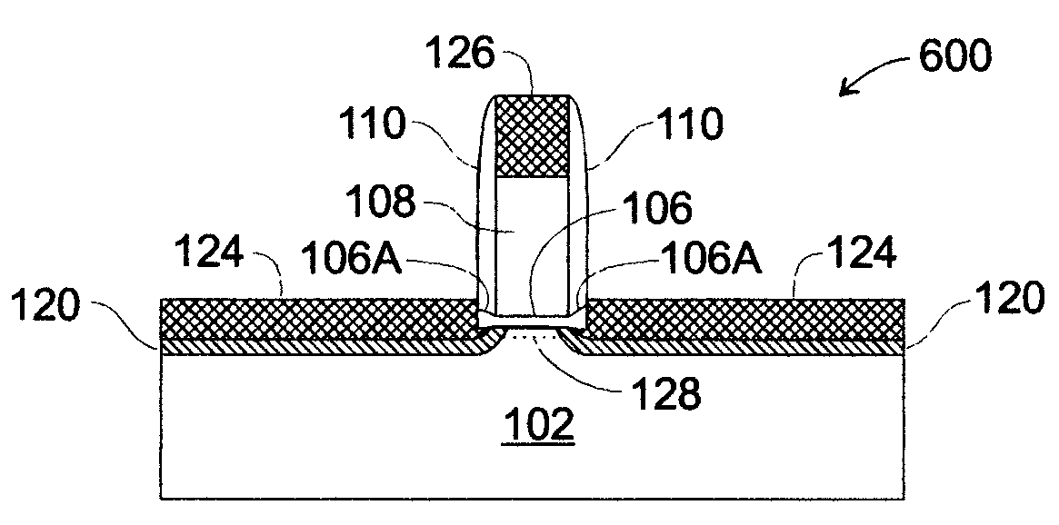
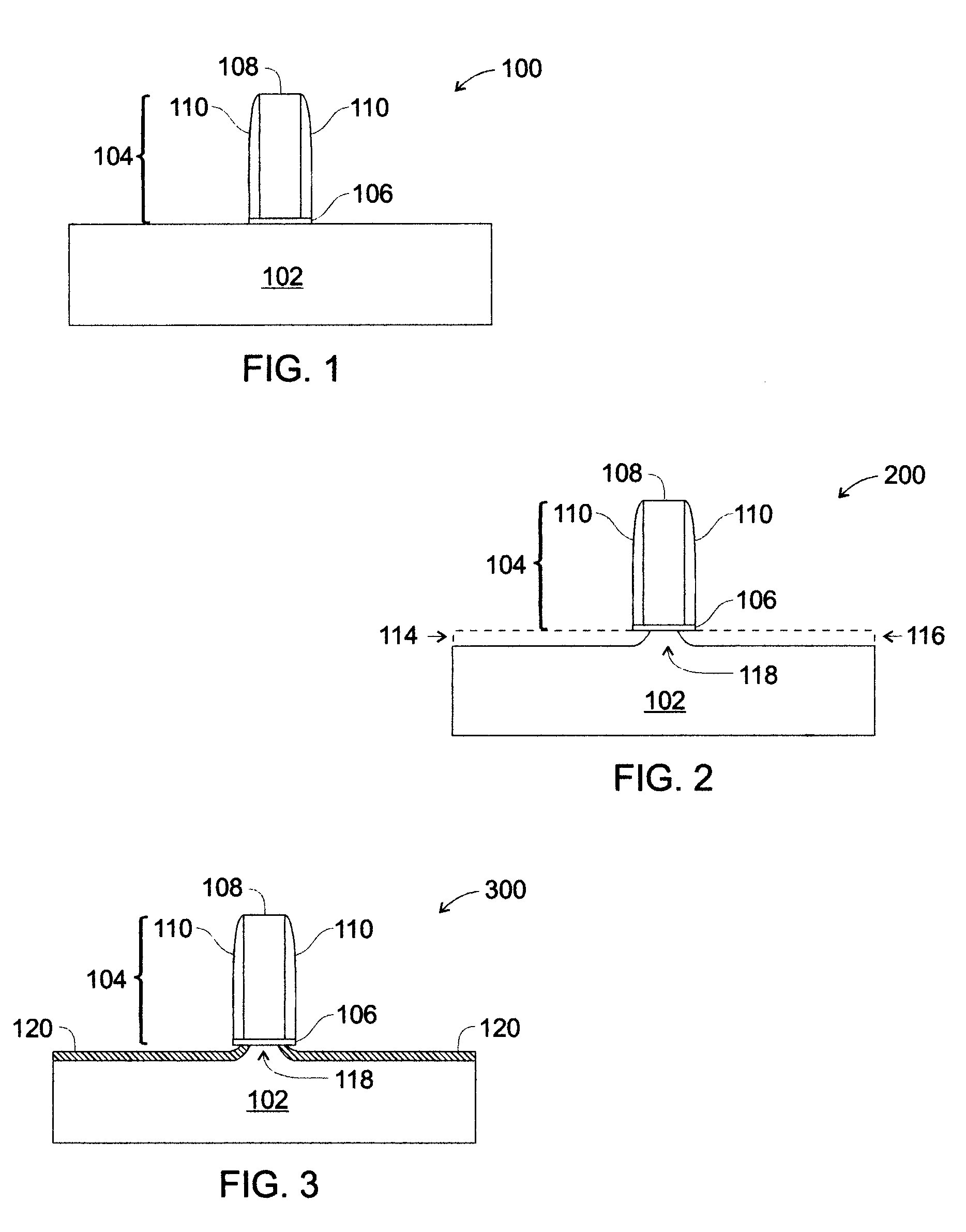
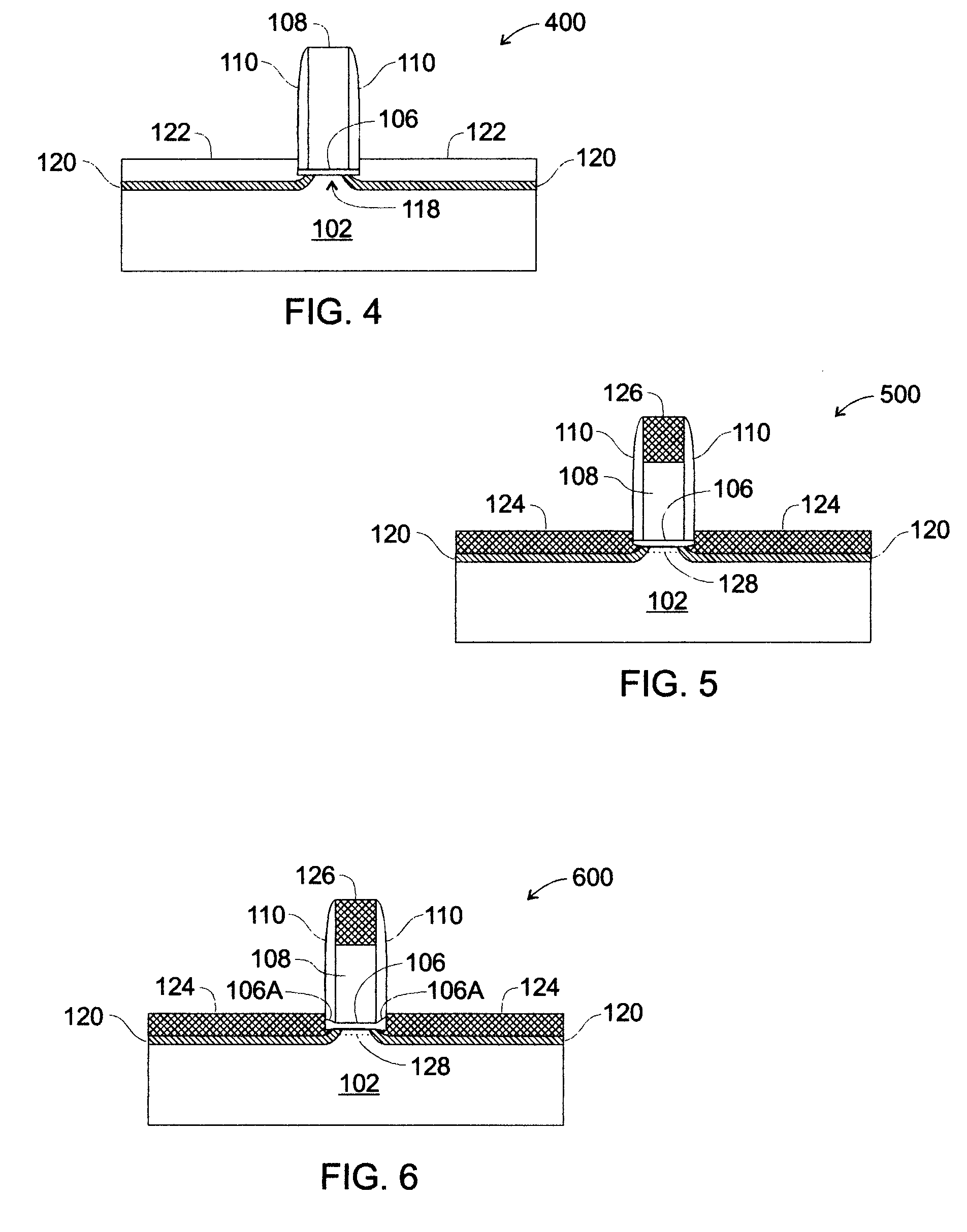
[0028] The present inventive technique produces MOSFET devices with low series resistance by replacing “traditionally” constructed source / drain extensions with very thin, highly-doped layers formed in an etched-away region that extends partially under the MOSFET's gate structure. These thin, highly-doped layers act both as silicidation stops and as source / drain lateral extensions. The etched-away regions in the active area adjacent to the thin lateral extension layers are then “filled” with a suitable silicide to complete the source / drain region of the MOSFET. As described in greater detail hereinbelow, the application of the thin lateral extension layers and the silicide in combination yields compact source / drain structures that exhibit very low series resistance.
[0029] Under conditions that would ordinarily be expected when forming suicides in doped silicon (using previously known techniques), the process of silicidation can be expected to produce lateral silicide expansion (grow...
PUM
| Property | Measurement | Unit |
|---|---|---|
| temperature | aaaaa | aaaaa |
| temperature | aaaaa | aaaaa |
| extension depth | aaaaa | aaaaa |
Abstract
Description
Claims
Application Information