Method of forming a contact plug in a semiconductor device

Inactive Publication Date: 2005-05-26
SK HYNIX INC
View PDF2 Cites 17 Cited by
  • Summary
  • Abstract
  • Description
  • Claims
  • Application Information

AI Technical Summary

Benefits of technology

[0013] Accordingly, the present invention has been made to solve the above-mentioned and other related problems occurring in the prior art. One object

Problems solved by technology

Excessively implanted ions cause gradual reduction of the refresh characteristics of the semiconductor device.
This diffusion of doped phosphorous causes deterioration of the refresh characteristics of the semiconductor device.
In particular, the phosphorous is diffused into the polysilicon material of the contact plug, thereby lowering the doping effect.
If defects, such as etching residues and natural oxides, exist between the surface of the substrate and the plug, the contact resistance may increase even if the epitaxial silicon is used for the plug, so it is difficult to obtain desired device characteristics.
The conventional pre-treatment process includes sequential performance of dry and wet cleaning processes and a hydrogen bake process (that is, a hydrogen heat-treatment process) under a high temperature condition above 800° C. Since the epitaxial silicon growth process is carried out at a temperature condition above

Method used


Image

  • Method of forming a contact plug in a semiconductor device
  • Method of forming a contact plug in a semiconductor device
  • Method of forming a contact plug in a semiconductor device

Examples


Embodiment Construction

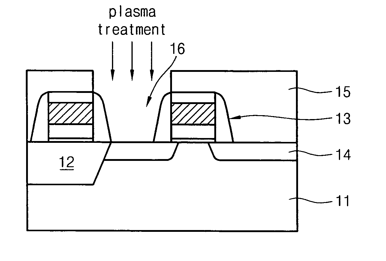
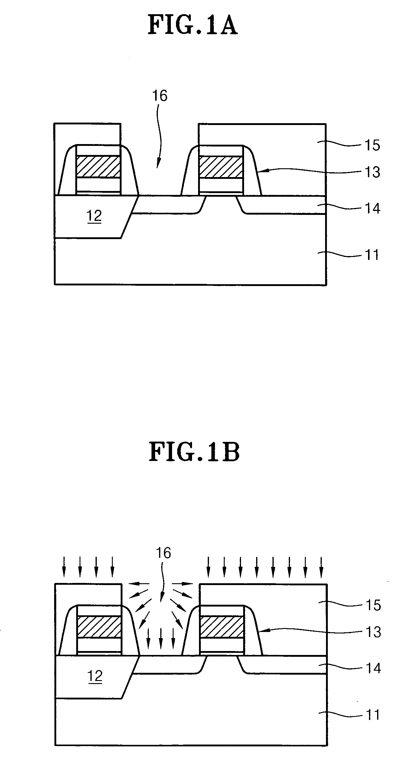
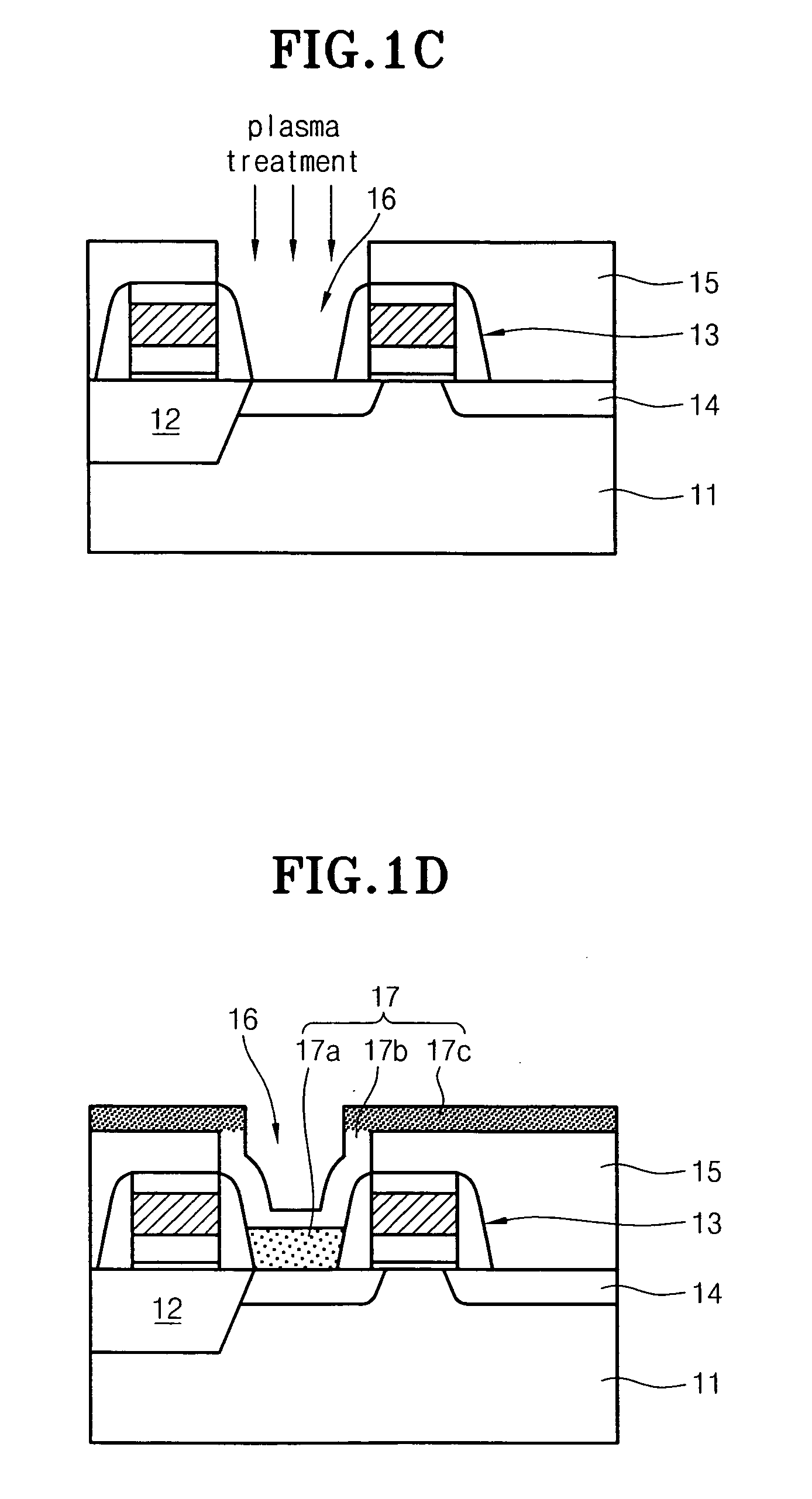
[0018] Generally, epitaxial silicon is used to make a contact plug in a semiconductor memory device to obtain a low contact resistance at a relatively low doping density. The lowered doping density allows small dopant diffusion.

[0019] According to an embodiment of the present invention, a hydrogen heat-treatment process, which is the conventional pre-treatment process requiring high temperature condition above 800° C., is replaced with a plasma treatment process requiring lower temperature condition, about 600° C. or lower. This lowers the thermal budget during the pre-treatment process and help to prevebt the device characteristic degradation.

[0020] Further according to an embodiment of the present invention particularly with respect to the SPE method of growing the epitaxial silicon, the amorphous silicon is deposited on the wafer in multiple deposition steps, i.e., at least more than two steps. A subsequent heat-treatment process allows the deposited amorphous silicon to be gro...


PUM


Abstract

A contact plug is formed in a semiconductor device having a silicon substrate having a gate electrode, a junction area and an insulating interlayer. A contact hole is formed to expose the junction area. A plasma process is carried out with respect to a resultant substrate, thereby removing natural oxides created on an exposed surface of the junction area. A first silicon layer is deposited on the contact hole and on the insulating interlayer. A heat-treatment process is carried out with respect to the first silicon layer so as to grow the amorphous silicon into the epitaxial silicon. A second silicon layer is deposited on the first silicon layer.

Description

BACKGROUND OF THE INVENTION [0001] 1. Field of the Invention [0002] The present invention relates generally to a method of forming a contact plug in a semiconductor device, and more particularly to a method of forming a contact plug in a semiconductor device that shortens heat-treatment time while minimizing degradation of the device characteristics due to high thermal budget. [0003] 2. Description of the Prior Art [0004] With increasing miniaturization of semiconductor devices, diffusion control of dopants is an important factor for preventing the thermal stress related degradation of refresh and other transistor characteristics. For example, the typically short gate length in a micro-size semiconductor device requires implanting of excessive ions in order to obtain the desired threshold voltage. Excessively implanted ions cause gradual reduction of the refresh characteristics of the semiconductor device. The doped ions, such as phosphorous (or the phosphorous ions), are known to d...

Claims


Application Information

Patent Timeline
IPC IPC(8): H01L21/285H01L21/3205H01L21/44H01L21/4763H01L21/768H01L21/8234H01L21/8244
CPCH01L21/28525H01L27/11H01L21/76877H10B10/00
Inventor PARK, SUNG EON
Owner SK HYNIX INC
Why Eureka
Try Eureka