Process for producing wafer

A manufacturing method and wafer technology are applied in the manufacture of epitaxial wafers, which can manufacture wafers at low cost and anneal the wafers, and can solve problems such as surface roughness, corrosion treatment equipment, and long time, so as to shorten the heat treatment process. effect of time, increased productivity, and reduced metal contamination

Inactive Publication Date: 2006-09-20
SHIN-ETSU HANDOTAI CO LTD
View PDF6 Cites 11 Cited by
  • Summary
  • Abstract
  • Description
  • Claims
  • Application Information

AI Technical Summary

Problems solved by technology

In addition, methods that can be implemented at around room temperature include wet etching using a dilute hydrofluoric acid solution, a combination of hydrogen fluoride gas and water vapor, and Ar plasma treatment. Surface roughness, corrosion treatment equipment and other problems, it is considered that the above-mentioned high temperature heat treatment is the most appropriate in the current situation
[0018] However, the gettering effect of the above-mentioned epitaxial wafer may not be sufficient
This is because the substrate that becomes the epitaxial wafer, after a high temperature step above 1000°C, the oxygen precipitation nuclei or oxygen precipitation products have almost been eliminated, and the function of getting gas cannot be achieved.
In the previous method, the pretreatment before epitaxial growth was not easy to fully remove the natural oxide film in the temperature range of less than 1000°C
Therefore, the pretreatment must be carried out at a temperature range above 1000°C, and the conventional method cannot avoid the reduction of the epitaxial wafer getter efficiency.
[0019] For this kind of substrate, in order to obtain the gettering effect, heat treatment for forming BMD must be performed before or after forming the epitaxial layer, which takes a long time

Method used


Image

  • Process for producing wafer
  • Process for producing wafer
  • Process for producing wafer

Examples


Embodiment 1

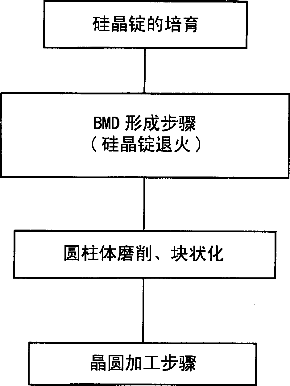
[0167] (Cultivation of silicon ingots)

[0168] By CZ method, the growth oxygen concentration is 13~15×10 17 atoms / cm 3 [oldASTM], the nitrogen concentration is 5~9×10 12 atoms / cm 3 silicon monocrystalline silicon ingot. The silicon ingot is cylindrically ground and cut into a plurality of silicon ingots to obtain a silicon ingot with a diameter of about 300 mm and a length of about 30 cm.

[0169] (Silicon ingot annealing: BMD formation step)

[0170] The above-mentioned silicon crystal ingot is heat-treated as it is in the state of the silicon crystal ingot, and a BMD forming step of forming a BMD inside is performed. First, use the HF / HNO 3 The formed acidic etchant performs about 200 micron etching to remove metal impurities that contaminate the surface.

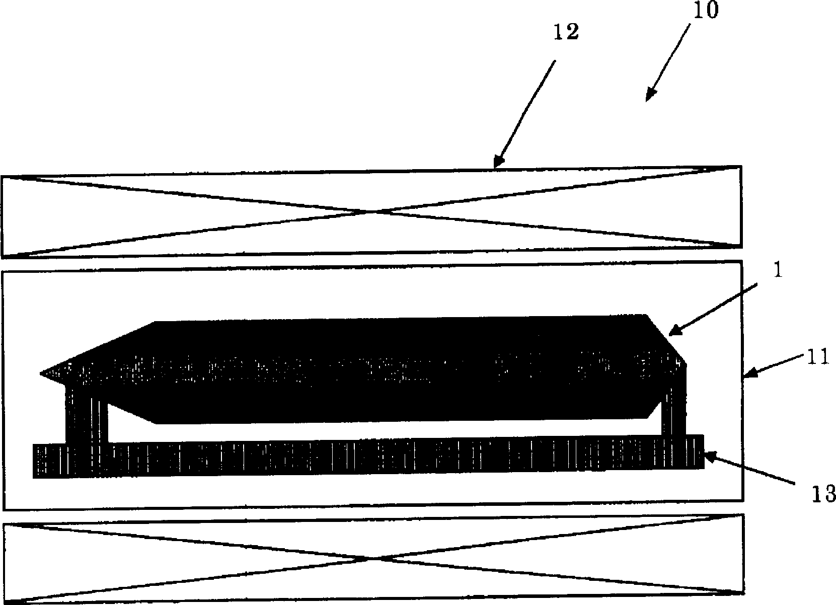
[0171] Next, in the state of the crystalline silicon ingot as it is, put Figure 4 Heat treatment is performed in the heat treatment furnace shown.

[0172] The heat treatment was carried out from room temperatu...

Embodiment 2

[0178] (Cultivation of silicon ingots)

[0179] By CZ method, the growth oxygen concentration is 13~15×10 17 atoms / cm 3 [oldASTM] silicon monocrystalline silicon ingot. This silicon single crystal is a crystal in which the NPC region is grown by controlling the crystal growth rate. By cutting the silicon crystal ingot into a plurality of silicon crystal blocks, a silicon crystal ingot with a diameter of about 300 mm and a length of about 30 cm was obtained.

[0180] Subsequently, in the same manner as in Example 1, the BMD formation step and wafer processing were performed to obtain about 300 silicon wafers with a diameter of 300 mm. As a result of evaluating the BMD density of the wafer thus obtained using infrared photography, it was 3×10 9 piece / cm 3 , with sufficient BMD density, wafers with high IG capability can be obtained.

Embodiment 3

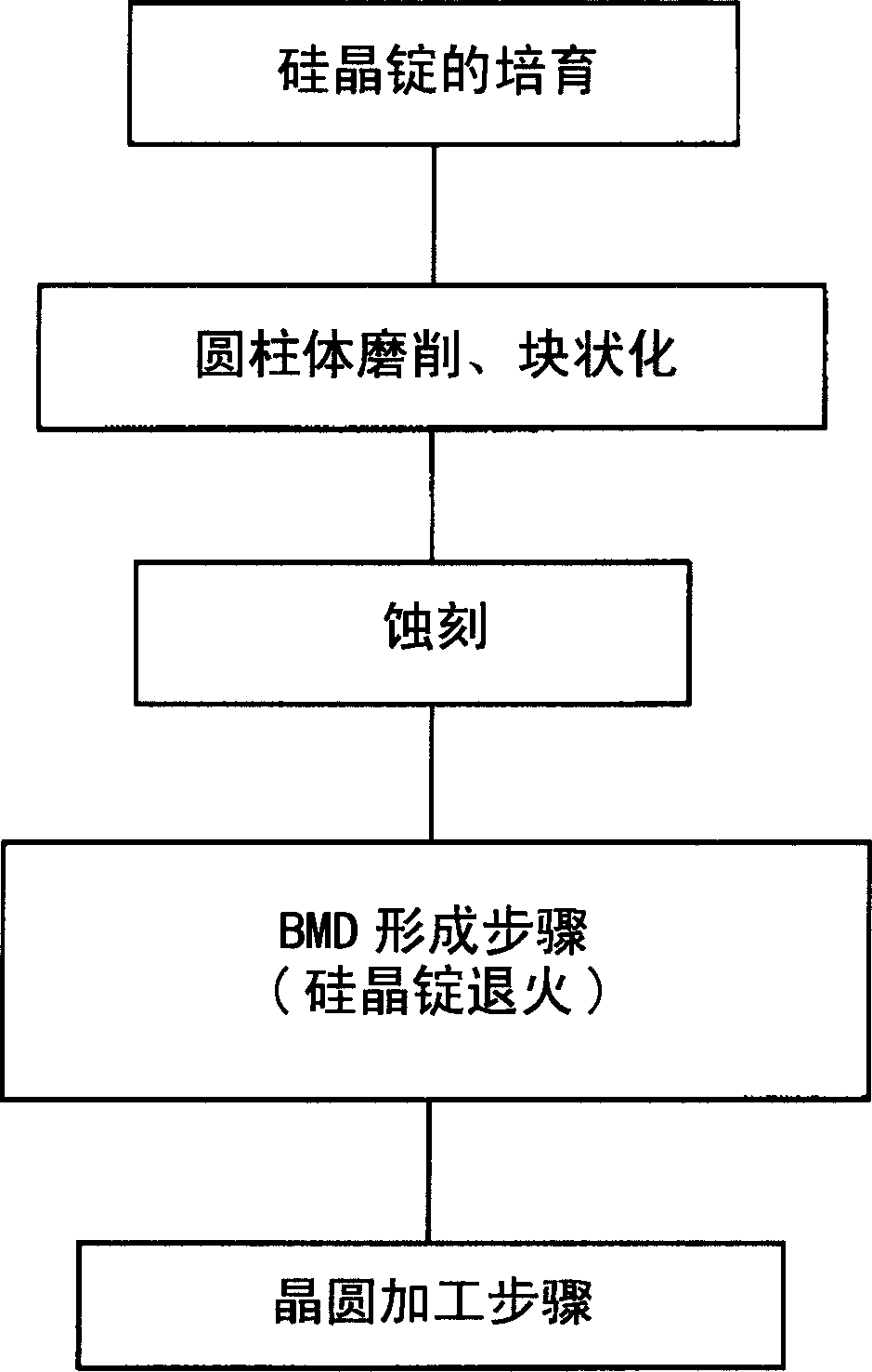
[0185] (Cultivation of silicon ingots)

[0186] By CZ method, the growth oxygen concentration is 13~15×10 17 atoms / cm 3 [oldASTM], the nitrogen concentration is 5~9×10 12 atoms / cm 3 silicon monocrystalline silicon ingot. The silicon ingot is cylindrically ground and cut into a plurality of silicon ingots to obtain a silicon ingot with a diameter of about 300 mm and a length of about 30 cm.

[0187] (Silicon ingot annealing: first heat treatment step)

[0188] To above-mentioned silicon crystal ingot, carry out the first heat treatment with the state of silicon crystal ingot as it is, at first, use by HF / HNO 3 The formed acidic etchant performs about 200 micron etching to remove metal impurities that contaminate the surface.

[0189] Next, in the state of the crystalline silicon ingot as it is, put Figure 4 Heat treatment is performed in the heat treatment furnace shown.

[0190] The heat treatment was carried out from room temperature to 500°C at a heating rate of 10°...


PUM

PropertyMeasurementUnit
lengthaaaaaaaaaa
diameteraaaaaaaaaa

Abstract

A process for producing a wafer, comprising at least the BMD formation step of subjecting a silicon single crystal having the form of an ingot to heat treatment to thereby form bulk microdefects (BMD) in the interior thereof, and the wafer machining step of machining the ingot furnished with the bulk microdefects (BMD) into a wafer. In this process for producing a wafer, the heat treatment for imparting IG capability in the wafer production can be shortened to thereby enable mass production of wafers of high IG capability. The process can further comprise the wafer heat treatment step of performing heat treatment of wafers after machining and the epitaxial growth step of forming an epitaxial layer on each of the wafers with the result that the productivity of, excelling in gettering effect, anneal wafers and epitaxial wafers can be enhanced.

Description

technical field [0001] The present invention relates to the manufacturing method of wafer, especially a kind of method that can manufacture wafer at low cost, and this wafer generates aerobic precipitate and internal tiny defect BMD ( Bulk Micro Defect). [0002] The present invention also relates to a method for manufacturing an annealed wafer, in particular to a method for manufacturing an annealed wafer. In order to form a DZ (Denuded Zone) layer of a defect-free zone on the surface, oxygen is carried out to the outside. Diffusion heat treatment and heat treatment to generate oxygen precipitates and internal microdefect BMD to impart IG capability. [0003] Furthermore, the present invention also relates to a method for manufacturing an epitaxial wafer, and more particularly relates to a method for efficiently manufacturing an epitaxial wafer having excellent gettering efficiency and few epitaxial layer defects. Background technique [0004] A silicon single crystal waf...

Claims


Application Information

Patent Timeline
Patent Type & Authority Applications(China)
IPC IPC(8): C30B29/06H01L21/322
Inventor 小林武史
Owner SHIN-ETSU HANDOTAI CO LTD
Why Eureka
Try Eureka