Method for producing a wafer

a wafer and processing method technology, applied in the direction of polycrystalline material growth, after-treatment details, etc., can solve the problems of reducing the ig capability of heat treatment for providing ig in the production of wafers, affecting the quality of the wafer, etc., to achieve high ig capability, reduce the effect of heat treatment and reducing the ig capability of producing wafers

Inactive Publication Date: 2006-07-13
SHIN-ETSU HANDOTAI CO LTD
View PDF0 Cites 29 Cited by
  • Summary
  • Abstract
  • Description
  • Claims
  • Application Information

AI Technical Summary

Benefits of technology

[0020] The first object of the present invention is to provide a method for producing a wafer wherein heat treatment for providing IG capability in producing the wafer can be reduced and wafers with high IG capability can be produced in large quantity.

Problems solved by technology

If by such heavy-metal contamination, defects or electrical levels are formed in the vicinity of a surface of the wafer, device characteristic is degraded.
In that case, it is anticipated that because of the temperature lowering of processes, it becomes difficult that BMDs are formed during the device processes.
Therefore, in a low temperature process, it becomes more difficult to obtain sufficient IG effect than that in a high temperature process.
Moreover, even if device processes are lowered in the temperature, it is difficult to avoid heavy-metal contamination by high-energy ion implantation and such, and therefore gettering technique is thought to be essential.
There are some cases that the oxide precipitates secondarily cause dislocations, stacking faults, or the like, by strain due to expansion of volume.
Therefore, in the case that such defects exist in the wafer surface and the device active layer, there is occasionally caused increase of leakage current, fault of oxide dielectric breakdown voltage, or the like.
Moreover, as devices come to have higher integration and become finer, Grown-in defects introduced in pulling a silicon single crystal by CZ method, which haven't been historically seen as a problem, significantly degrade oxide dielectric breakdown voltage characteristic.
However, annealing as described above, which is referred to as DZ-IG heat treatment, requires much time because a wafer is subjected to two-step heat treatment having the different purposes of DZ layer formation and BMD formation.
However, the number of wafers able to be set therein is limited to at most about one hundred.
However, as a wafer has a larger diameter, such an apparatus for performing heat treatment also becomes larger and a heat treatment boat used for it and such also become larger, and thus very expensive apparatuses become required in terms of equipment.
Therefore, there is cost limitation for introducing many apparatuses, it is more important to effectively operate a heat treatment apparatus.
However, there are problems such as regrowth of an oxide film immediately after the treatment, occurrence of surface roughness of a substrate, and corrosion of treatment equipment.
However, as for an epitaxial wafer as described above, there are some cases that gettering effect is not sufficient.
In a conventional method, by the pretreatment before the epitaxial growth, it is difficult to sufficiently remove a native oxide film in a temperature zone of less than 1000° C. Therefore, the pretreatment cannot help but being performed in a temperature zone of 1000° C. or more.
Accordingly, it was impossible to avoid lowering of gettering efficiency of an epitaxial wafer, conventionally.

Method used


Image

  • Method for producing a wafer
  • Method for producing a wafer
  • Method for producing a wafer

Examples


example 1

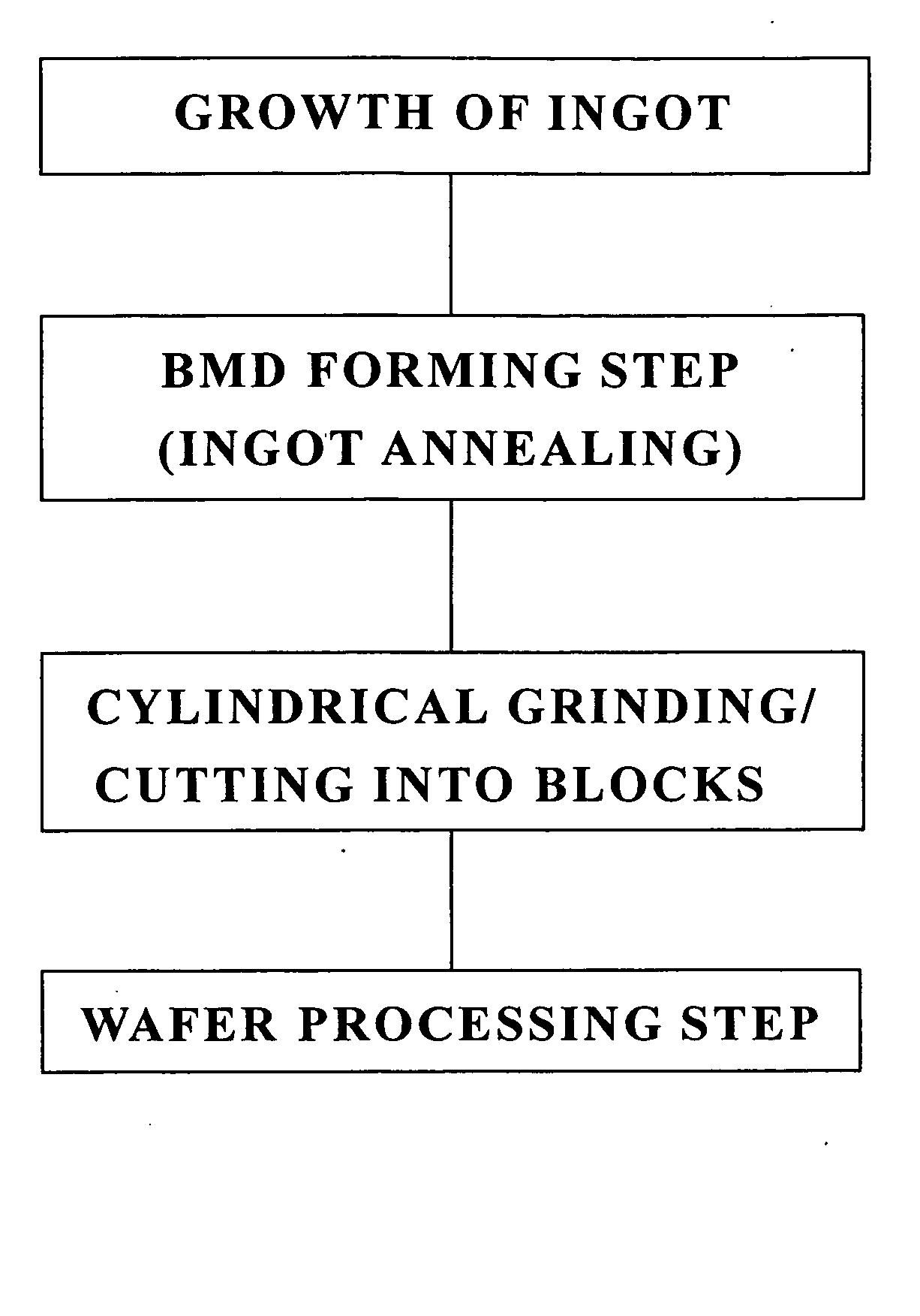
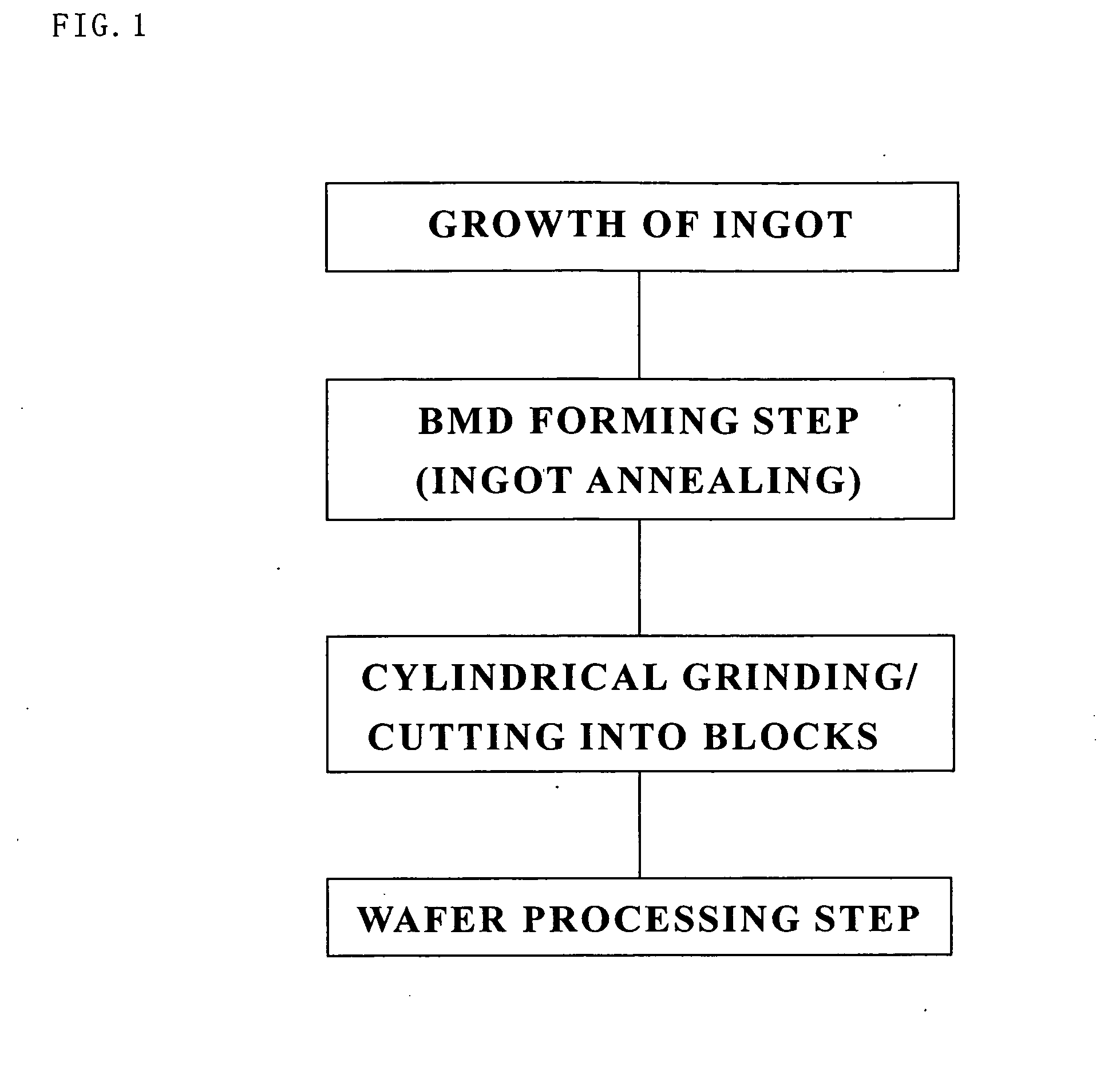
[0142] A silicon single crystal ingot with an oxygen concentration of 13-15×1017 atoms / cm3 [oldASTM] and with a nitrogen concentration of 5-9×10¹² atoms / cm3 was grown by CZ method. This ingot was cylindrically ground and cut into a plurality of blocks and thereby an ingot with a diameter of about 300 mm and with a length of about 30 cm was obtained.

[0143] A BMD forming step of subjecting the above ingot to heat treatment in a state of an ingot as it is to form BMDs inside was performed. First, the entire surface of the ingot was etched by about 200 μm by an acidic etchant consisting of HF / HNO3, and thereby metal impurity contaminating a surface thereof was removed.

[0144] After that, the ingot was put in the heat-treating furnace as shown in FIG. 4 in a state of an ingot as it is, and heat treatment was performed.

[0145] The heat treatment was performed that temperature was raised from the room temperature to 500° C. at a temperature rising rate of 10° C. / min, then raised to 1000° ...

example 2

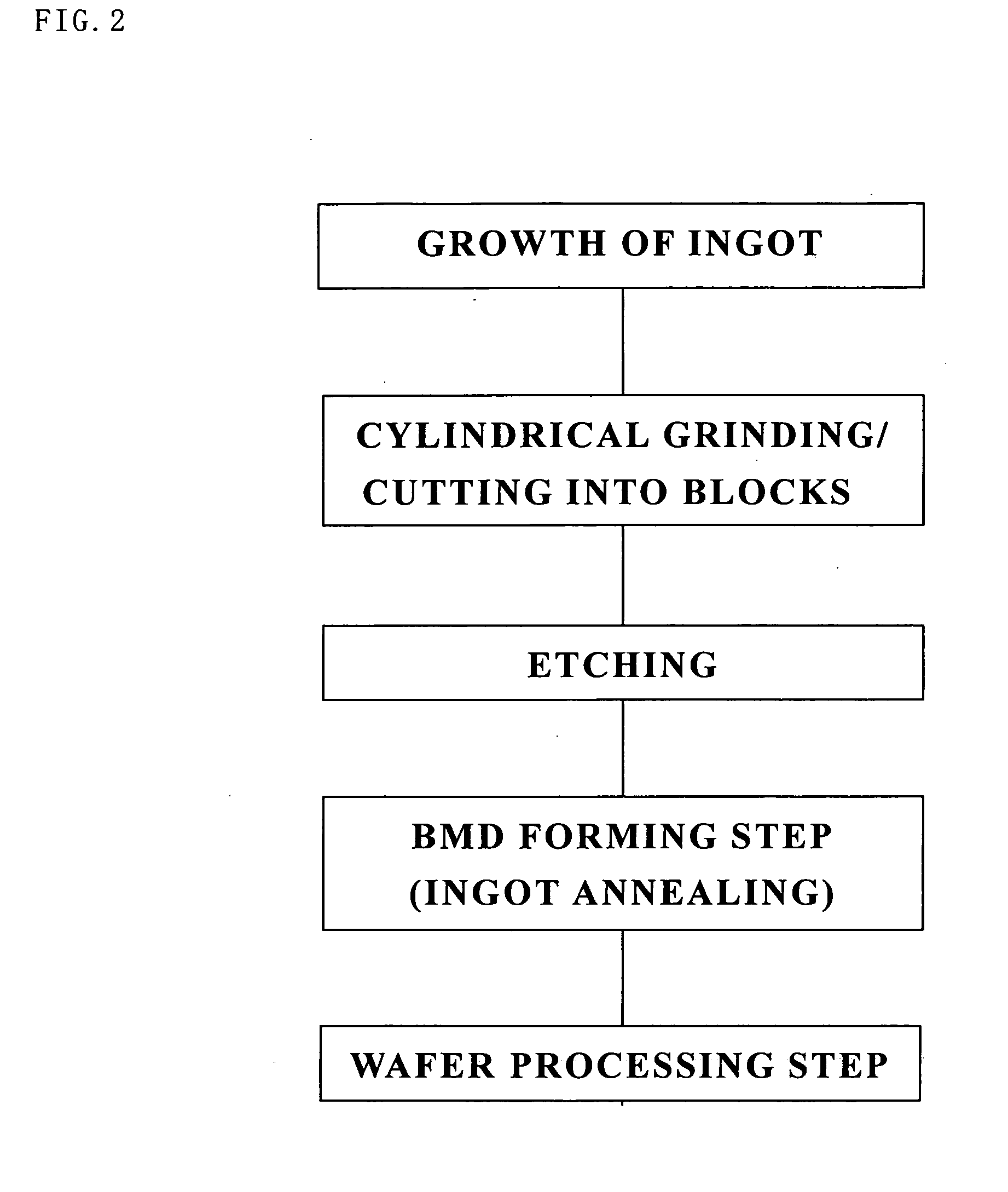
[0149] A silicon single crystal ingot with an oxygen concentration of 13-15×1017 atoms / cm3 [oldASTM] was grown by CZ method. With regard to the silicon single crystal, a crystal in NPC region was grown by controlling a growth rate of the crystal. The ingot was cylindrically ground and cut into a plurality of blocks, and thereby an ingot with a diameter of about 300 mm and with a length of about 30 cm was obtained.

[0150] After that, by performing BMD forming step and wafer processing step in the same manner as Example 1, about 300 silicon wafers with a diameter of 300 mm were obtained. With regard to the wafers obtained as described above, BMD density was evaluated by an infrared tomographic method. The result was a sufficient BMD density of 3×10⁹ numbers / cm3. Thus, wafers with high IG capability were obtained.

example 3

[0153] A silicon single crystal ingot with an oxygen concentration of 13-15×1017 atoms / cm3 [OldASTM] and with a nitrogen concentration of 5-9×10¹² atoms / cm3 was grown by CZ method. This ingot was cylindrically ground and cut into a plurality of blocks and thereby an ingot with a diameter of about 300 mm and with a length of about 30 cm was obtained.

[0154] The above ingot was subjected to the first heat-treating step in a state of an ingot as it is. First, the entire surface of the ingot was etched by about 200 μm by an acidic etchant consisting of HF / HNO3, and thereby metal impurity contaminating a surface thereof was removed.

[0155] After that, the ingot in a state of an ingot was put in the heat-treating furnace as shown in FIG. 4 as it is, and heat treatment was performed.

[0156] The heat treatment was performed that temperature was raised from the room temperature to 500° C. at a temperature rising rate of 10° C. / min, then raised to 1000° C. at a temperature rising rate of 1° C...


PUM

PropertyMeasurementUnit
temperatureaaaaaaaaaa

Abstract

The present invention is a method for producing a wafer comprising, at least, a BMD forming step of subjecting a silicon single crystal in a state of an ingot to heat treatment thereby to form bulk micro defects (BMDs) inside, and a wafer processing step of processing the ingot in which the bulk micro defects (BMDs) was formed into wafers. Thereby, there can be provided a method for producing a wafer, wherein heat treatment for providing IG capability in production of wafer can be shortened and wafers with high IG capability can be produced in large quantity. Also, the present invention can further comprise a wafer heat-treating step of subjecting the processed wafer to heat treatment, or an epitaxial growth step of forming an epitaxial layer on the wafer. Thereby, there is improved productivity of annealed wafers or epitaxial wafers that are excellent in gettering capability.

Description

TECHNICAL FIELD [0001] The present invention relates to a method for producing a wafer, particularly a method for producing at low cost a wafer in which oxide precipitates and bulk micro defects (BMDs) are generated for providing Intrinsic Gettering (IG) capability. [0002] Moreover, the present invention relates to a method for producing an annealed wafer, particularly, a method for producing an annealed wafer, wherein an oxygen out-diffusion heat treatment for forming a DZ (Denuded Zone) layer, which is a defect-free region, in the surface, and an heat treatment for generating oxide precipitates and bulk micro defects (BMDs) for providing IG capability are performed. [0003] Furthermore, the present invention relates to a method for producing an epitaxial wafer, particularly, a method for effectively producing an epitaxial wafer that is excellent in gettering effect and has few defects of the epitakial layer. BACKGROUND ART [0004] A silicon single crystal wafer used as a substrate o...

Claims


Application Information

Patent Timeline
Patent Type & Authority Applications(United States)
IPC IPC(8): C30B23/00C30B25/00C30B28/12C30B28/14C30B29/06C30B33/02
CPCC30B29/06C30B33/02
Inventor KOBAYASHI, TAKESHI
Owner SHIN-ETSU HANDOTAI CO LTD
Why Eureka
Try Eureka