Method of crystallizing amorphous semiconductor thin film and method of fabricating poly crystalline thin film transistor using the same

a technology of amorphous semiconductors and thin films, which is applied in the direction of crystal growth process, polycrystalline material growth, chemistry apparatus and processes, etc., can solve the problems of deteriorating an electrical feature of a device, long processing time, and long heat treatment time necessary for crystallization, etc., and achieves high speed, easy formation, and high speed

Inactive Publication Date: 2006-06-08
PAIK WOON SUH
View PDF5 Cites 11 Cited by
  • Summary
  • Abstract
  • Description
  • Claims
  • Application Information

AI Technical Summary

Benefits of technology

[0022] To solve the above problems, it is an object of the present invention to provide a method of crystallizing an amorphous semiconductor thin film which can reduce a total of heat treatment time of a thin film transistor, by primarily heat treating a source / drain before impurities are doped into the source / drain in order to perform primary crystallization, and doping the impurities into the source / drain to then perform secondary crystallization.
[0023] It is another object of the present invention to provide a method of crystallizing an amorphous semiconductor thin film which prevents a surface roughness from worsening and a trap site from being formed due to a mechanical stress between a semiconductor layer and a gate insulation film and can reduce a total of heat treatment time of a thin film transistor, by crystallizing the entire semiconductor layer at the time of a primary heat treatment before impurities are doped and activating the injected impurities at the time of a secondary heat treatment after the impurities have been doped.
[0024] It is still another object of the present invention to provide a method of crystallizing an amorphous semiconductor thin film using a MILC (Metal Induced Lateral Crystallization) method which can prevent a remaining crystallization induced metal which is not changed into silicide from diffusing onto a semiconductor thin film surface being an operational region of a transistor, by forming a MILC crystallization induced metal is formed on a substrate in advance before an amorphous semiconductor thin film is formed.

Problems solved by technology

Meanwhile, since according to one published paper, metal pollution occurring due to a crystallization induced metal deposited on the silicon surface for the conventional MILC exists in the channel region of the poly-crystalline thin film transistor, it has been reported that a problem for deteriorating an electrical feature of a device has been known (see IEEE Trans.
Thus, when an N-type poly-crystalline thin film transistor is fabricated, a heat treatment time necessary for crystallization becomes very long.
Accordingly, in the case of a CMOS (Complementary Metal-Oxide Semiconductor) device where N-type and P-type thin film transistors to be widely used for a display driving IC (Integrated Circuit) exist simultaneously, a processing time becomes long and thus a processing cost increases when a poly-crystalline thin film transistor device is fabricated.

Method used


Image

  • Method of crystallizing amorphous semiconductor thin film and method of fabricating poly crystalline thin film transistor using the same
  • Method of crystallizing amorphous semiconductor thin film and method of fabricating poly crystalline thin film transistor using the same
  • Method of crystallizing amorphous semiconductor thin film and method of fabricating poly crystalline thin film transistor using the same

Examples


first embodiment

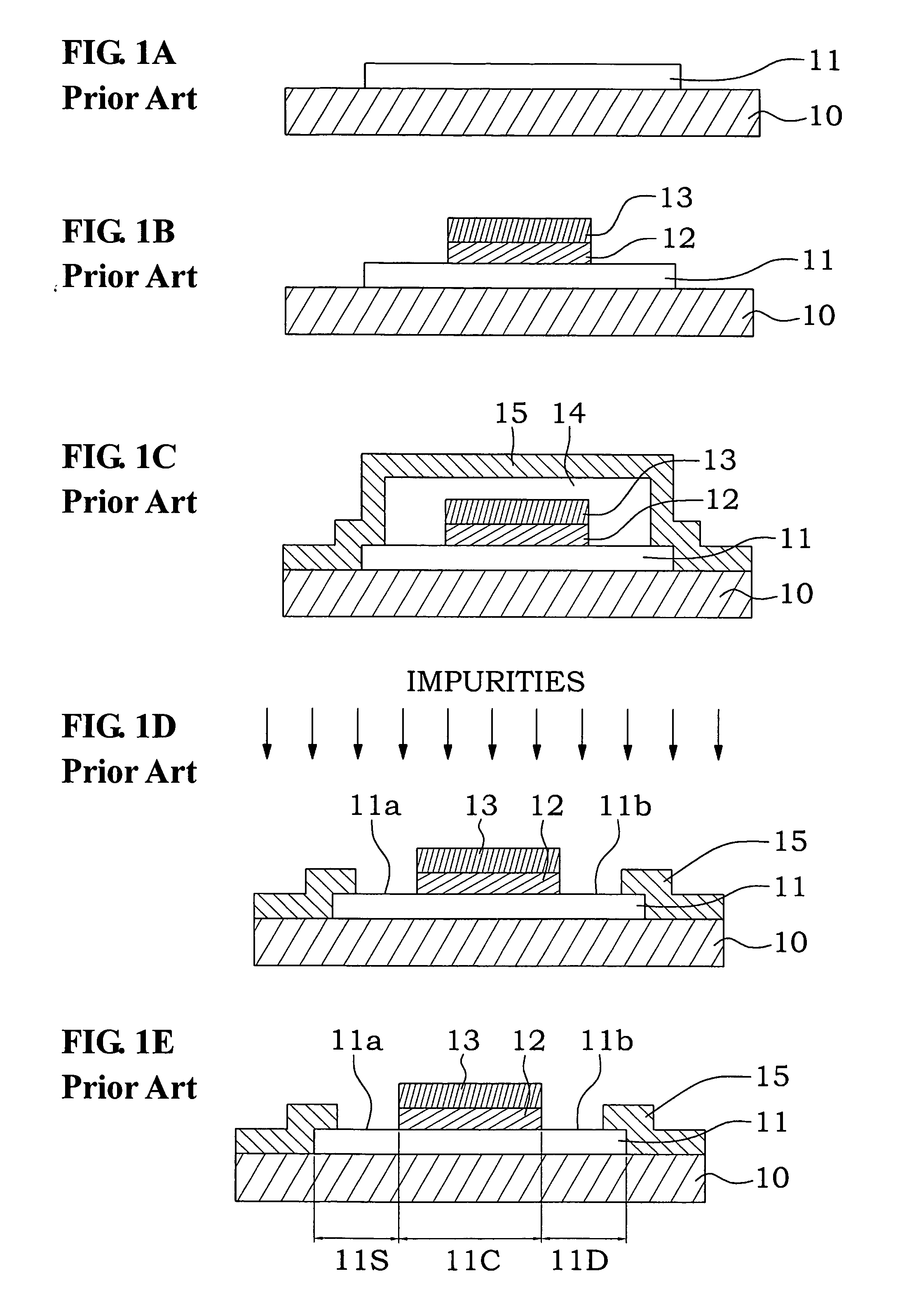
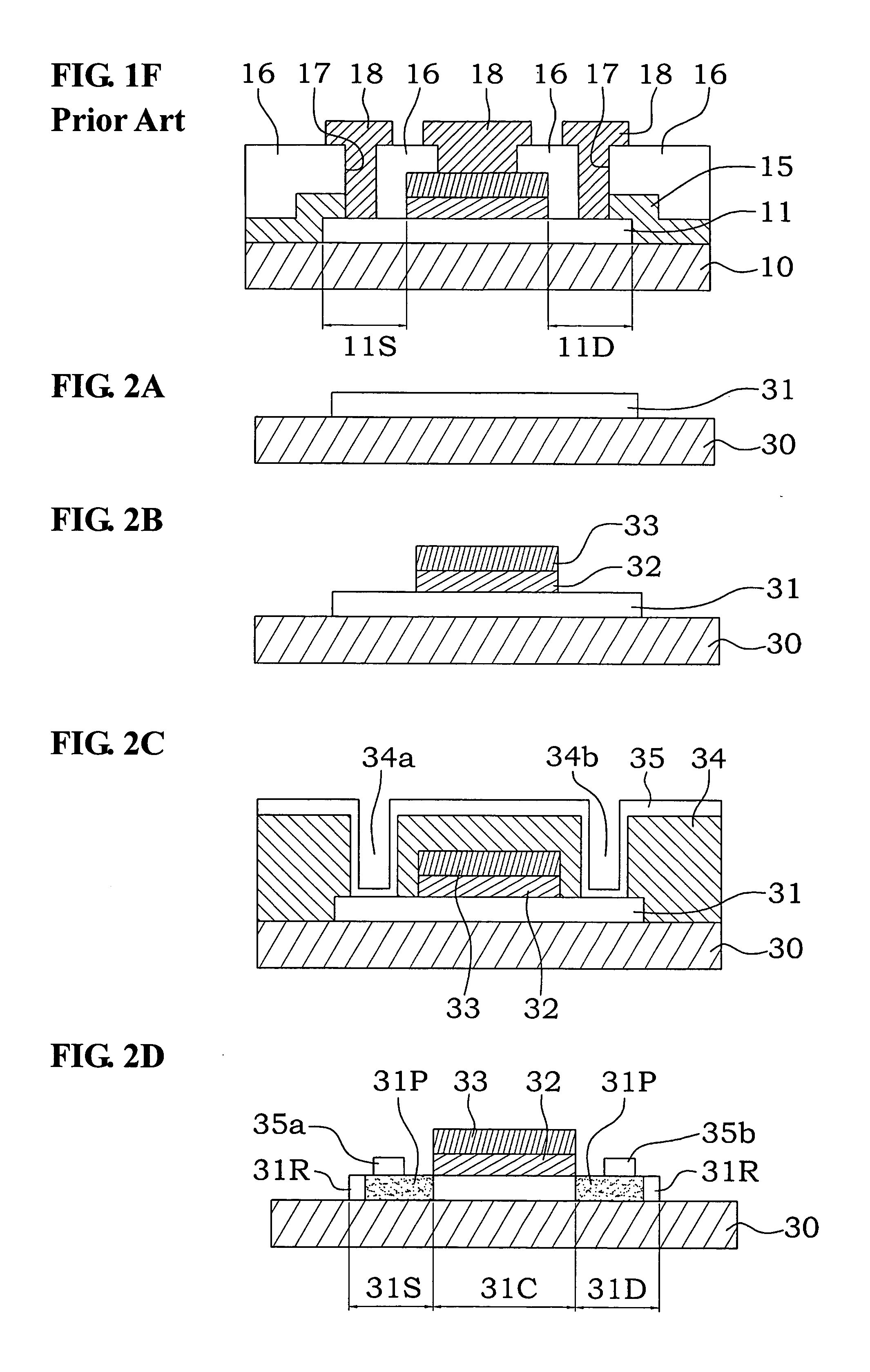
[0073] As a result, it is possible to use seeds of MILC metal films using the contact method even at the time of fabrication of the N-type TFT in the present invention. Accordingly, in the present invention, a separate mask does not need to be fabricated in order to form seeds of the MILC metal films 35a and 35b, but a contact mask which is essentially fabricated in order to form a contact window with respect to the source and drain regions is used for fabricating a thin film transistor (TFT), to thereby form a photosensitive film pattern 34 having contact holes 34a and 34b with respect to the source and drain regions.

[0074] Further, in the case of the conventional heat treatment method, boron (B) such as B2H4, or phosphorus (P) such as PH3 are doped into portions where the source and drain regions of a semiconductor layer made of amorphous silicon, and then crystallization of the amorphous silicon and activation of the impurities are simultaneously accomplished at a one-time crysta...

second embodiment

[0081] Hereinbelow, a method of fabricating a thin film transistor using a MILC method according to the present invention will be described with reference to FIGS. 4A through 4G.

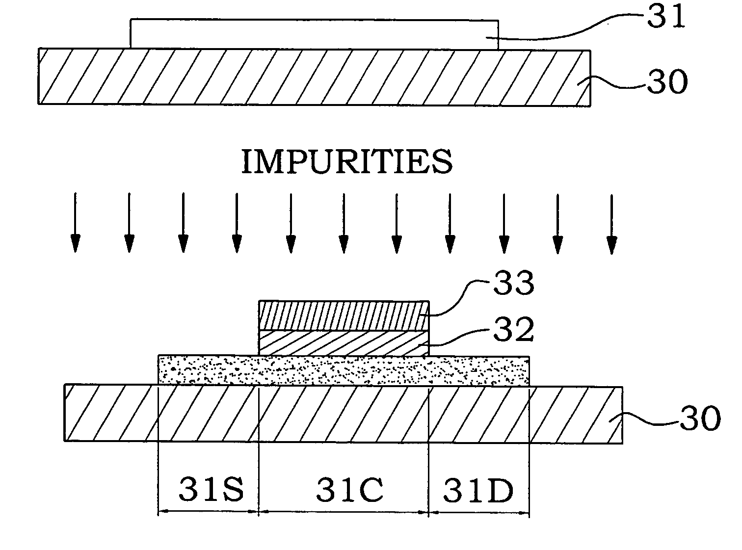
[0082] Referring to FIG. 4A, an amorphous silicon thin film is deposited on a transparent insulation substrate 40, through a CVD (Chemical Vapor Deposition) or sputtering method and then patterned using a mask (not shown) for forming a semiconductor layer, to thereby form a semiconductor layer 41.

[0083] Then, as shown in FIG. 4B, a photosensitive film pattern 42 having contact holes 42a and 42b with respect to a source region and a drain region is formed on the substrate 40 using a mask (not shown), and then a MILC metal film 43 is deposited on the entire surface of the substrate 40. As a result, the MILC metal film 43 contacts partially the source and drain regions via the contact holes 42a and 42b.

[0084] The MILC metal film 43 is deposited with a thickness of 10˜10,000 Å, preferably, 10˜200 Å, on the ins...

third embodiment

[0098] Hereinbelow, a method of fabricating a thin film transistor using a MILC method according to the present invention will be described with reference to FIGS. 5A through 5F.

[0099] Referring to FIG. 5A, a photosensitive film is deposited on a transparent insulation substrate 50, and then patterned using a mask (not shown), to thereby form a photosensitive film pattern 51 in which first and second contact holes 51a and 51b for the source and drain reservation regions are disposed at a predetermined interval.

[0100] Then, a MILC metal film 52 is deposited on the entire surface of the substrate 40 where the photosensitive film pattern 51 has been formed. As a result, the MILC metal film 52 contacts partially the source and drain reservation regions via the contact holes 51a and 51b.

[0101] The MILC metal film 52 is deposited with a thickness of 10˜10,000 Å, preferably, 10˜200 Å, on the insulation substrate 40, by any one of sputtering, evaporation by heating, PECVD (Plasma Enhanced...


PUM

PropertyMeasurementUnit
temperatureaaaaaaaaaa
temperaturesaaaaaaaaaa

Abstract

A method of crystallizing an amorphous semiconductor thin film used for a thin film transistor (TFT) is provided. The method includes the steps of: forming first and second crystallization induced metal patterns locally in respective portions of a source region and a drain region of the TFT on an amorphous semiconductor thin film; and crystallizing an amorphous semiconductor via independent two-times heat treatment using the first and second crystallization induced metal patterns. In this case, the independent two-times heat treatment is executed before and after ions of impurities are injected, respectively. In this way, a metal induced lateral crystallization double heat treatment is executed before and after ions of impurities are injected, respectively. As a result, the entire crystallization heat treatment time necessary for crystallizing the amorphous semiconductor thin film can be greatly reduced, and a poly-crystalline TFT having low leakage current can be obtained.

Description

BACKGROUND OF THE INVENTION [0001] 1. Field of the Invention [0002] The present invention relates to a method of crystallizing an amorphous semiconductor thin film, and a method for fabricating a poly-crystalline thin film transistor using the same, and more particularly, to a method of crystallizing an amorphous semiconductor thin film, and a method for fabricating a poly-crystalline thin film transistor using the same, in which independent two-times heat treatments are executed before and after impurities are ion-injected when a low-temperature poly-crystalline thin film transistor is fabricated via a metal induced lateral crystallization method or the other corresponding methods, to thereby shorten a heat treatment time. [0003] 2. Description of the Related Art [0004] In general, a thin film transistor which is used in a display device such as a liquid crystal display (LCD) or an organic light emitting diode (OLED) is fabricated by processes of depositing an amorphous semiconduct...

Claims


Application Information

Patent Timeline
Patent Type & Authority Applications(United States)
IPC IPC(8): H01L21/00H01L21/36H01L21/20C30B1/00H01L21/84
CPCC30B13/00C30B29/06H01L21/2022H01L29/66757H01L29/78675H01L21/02667H01L21/02532H01L21/02672H01L27/1277
Inventor PAIK, WOON SUH
Owner PAIK WOON SUH
Why Eureka
Try Eureka