Eureka AIR delivers breakthrough ideas for toughest innovation challenges, trusted by R&D personnel around the world.

Low-overhead processor interfacing

a processor and low-overhead technology, applied in the field of low-overhead processor interfacing, can solve the problems of high interrupt overhead and associated dsp core load, shared memory system may have difficulty in ensuring latency, and performance will be poor, so as to reduce interrupt overhead and associated core load

Inactive Publication Date: 2005-05-26
NOKIA SOLUTIONS & NETWORKS OY
View PDF4 Cites 10 Cited by
  • Summary
  • Abstract
  • Description
  • Claims
  • Application Information

AI Technical Summary

Benefits of technology

[0007] It is therefore an object of the present invention to provide a method and system for transferring data between a memory of a processor device and a circuitry connected to the processor device, by means of which interrupt overheads and associated core load can be reduced.
[0018] Accordingly, a pre-programmed DMA located on interfaces hosted by the external circuitry is provided to transfer data between the memory and the external circuitry, wherein processor control requirements can be reduced by using the transaction log. Thus, a plurality of data transfers can be bundled with a single DMA operation, since the processor device may validate or qualify the transferred data based on the available transaction log, when the availability, e.g. transfer or interrogation, of the transaction log has been informed to the processor device. Since the processor device is only involved in the signaling of the information regarding the provision, e.g. transfer or interrogation, of the transaction log, interrupt overheads and associated core load can be significantly reduced. Furthermore, the need for manual data movement is prevented, and a data rate matching can be provided between the shared memory and the on-chip bus system of the external circuitry to thereby reduced stalling of the system.
[0019] Due to the fact that multiple data structures held in the memory can be validated using a single processor involvement, e.g. by an interrupt service routine, core processing overhead is reduced especially when context switching is required under a real-time operating system (RTOS). Furthermore, since the transaction log can be stored locally within the memory of the processor device, slow core polling of the transaction status within the external circuitry is not required. Significant background data movements are therefore allowed between the shared memory and the external circuitry, because means are provided for synchronizing and validating the data structures without high core overheads.

Problems solved by technology

Shared memory systems may have difficulties in guaranteeing latency due to the uncertainties over memory contention.
If the central processing unit (CPU) of a DSP has to stop its current task and move data on and off the chip, performance will be poor.
Thus, high interrupt overheads and associated DSP core load are associated with frequent interrupt service routines (ISRs) triggered in case of data movements between the shared memory and external devices or circuitries connected to the DSP.
However, if this prior art solution is used for bundling interrupts of data movements between a shared memory of a DSP and an external circuitry, the CPU of the DSP still has to handle each interrupt of the interrupt block in order to trigger the corresponding ISRs required for data movement.
Hence, overhead would still be a problem.

Method used


Image

  • Low-overhead processor interfacing
  • Low-overhead processor interfacing
  • Low-overhead processor interfacing

Examples


Embodiment Construction

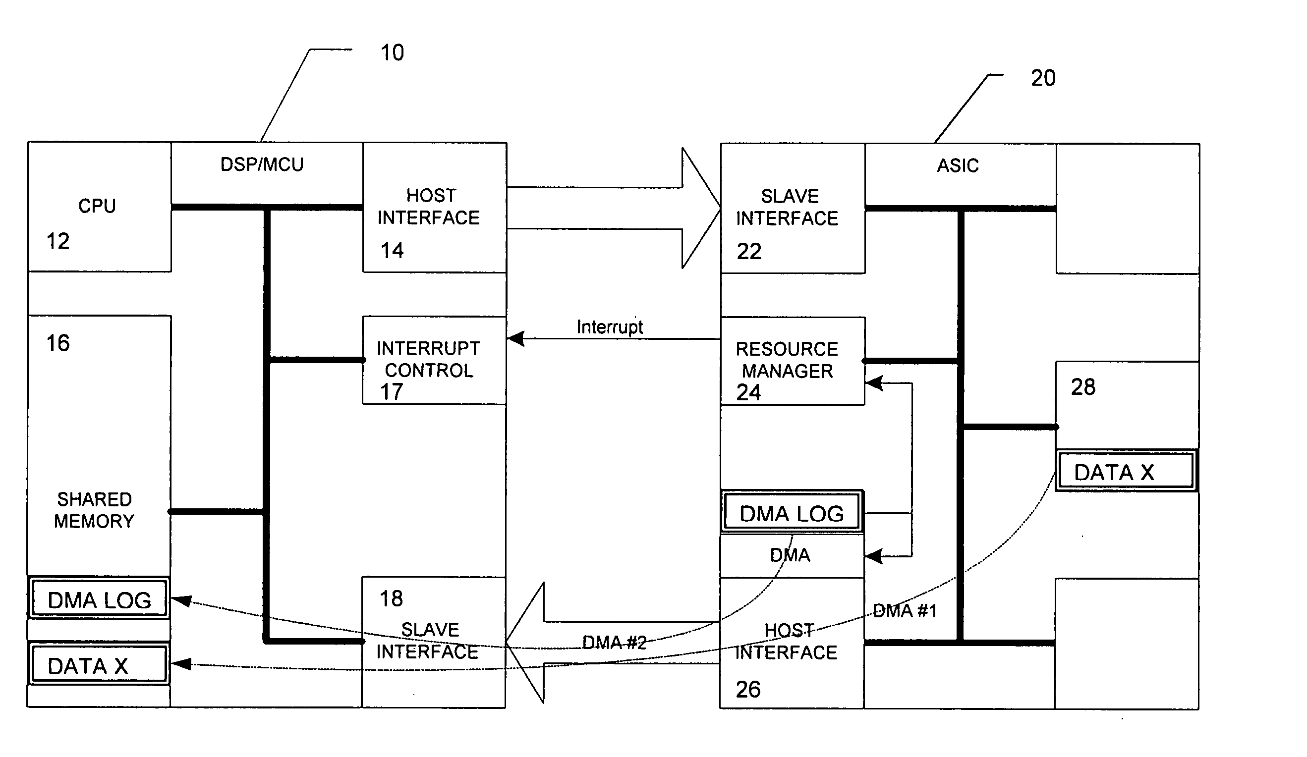
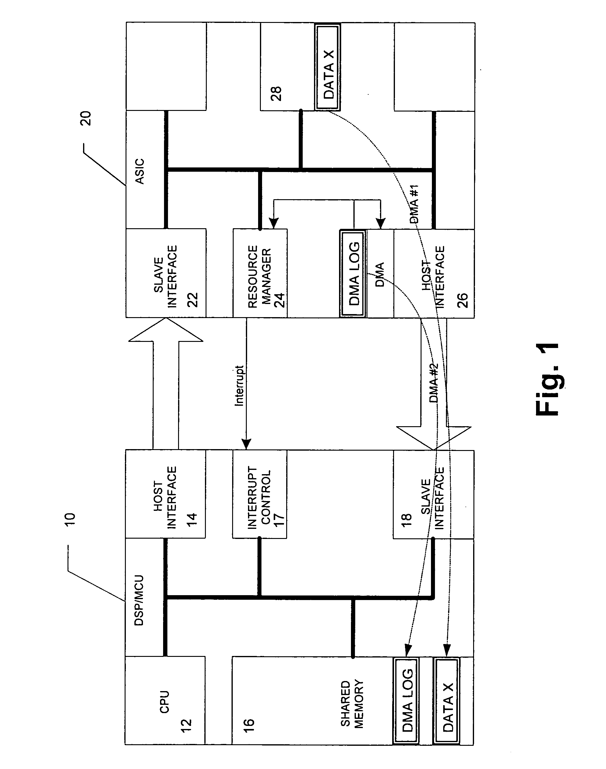
[0026] The preferred embodiment will now be described based on a pre-programmed DMA located on an ASIC-hosted interface to provide a data movement between a shared memory 16 of a DSP or Microcontroller Unit (MCU) 10 and an ASIC 20, as shown in FIG. 1.

[0027] According to FIG. 1, the DSP 10 comprises a CPU 12 for controlling DSP operations based on a control program stored in a program memory (not shown). Furthermore, a host interface 14 is provided for controlling a data transfer to a slave interface 22 arranged at the ASIC 20. An interrupt control unit 17 is arranged in the DSP 10 to control the execution of interrupt service routines based on an interrupt control signal received from a resource manager 24 of the ASIC 20. Moreover, a slave interface 18 of the DSP 10 is controlled by a host interface 26 of the ASIC 20 so as to transfer data from the ASIC 20 to the shared memory 16 of the DSP 10.

[0028] In the ASIC 20, a memory 28 is provided for storing data to be transferred e.g. t...


PUM


Abstract

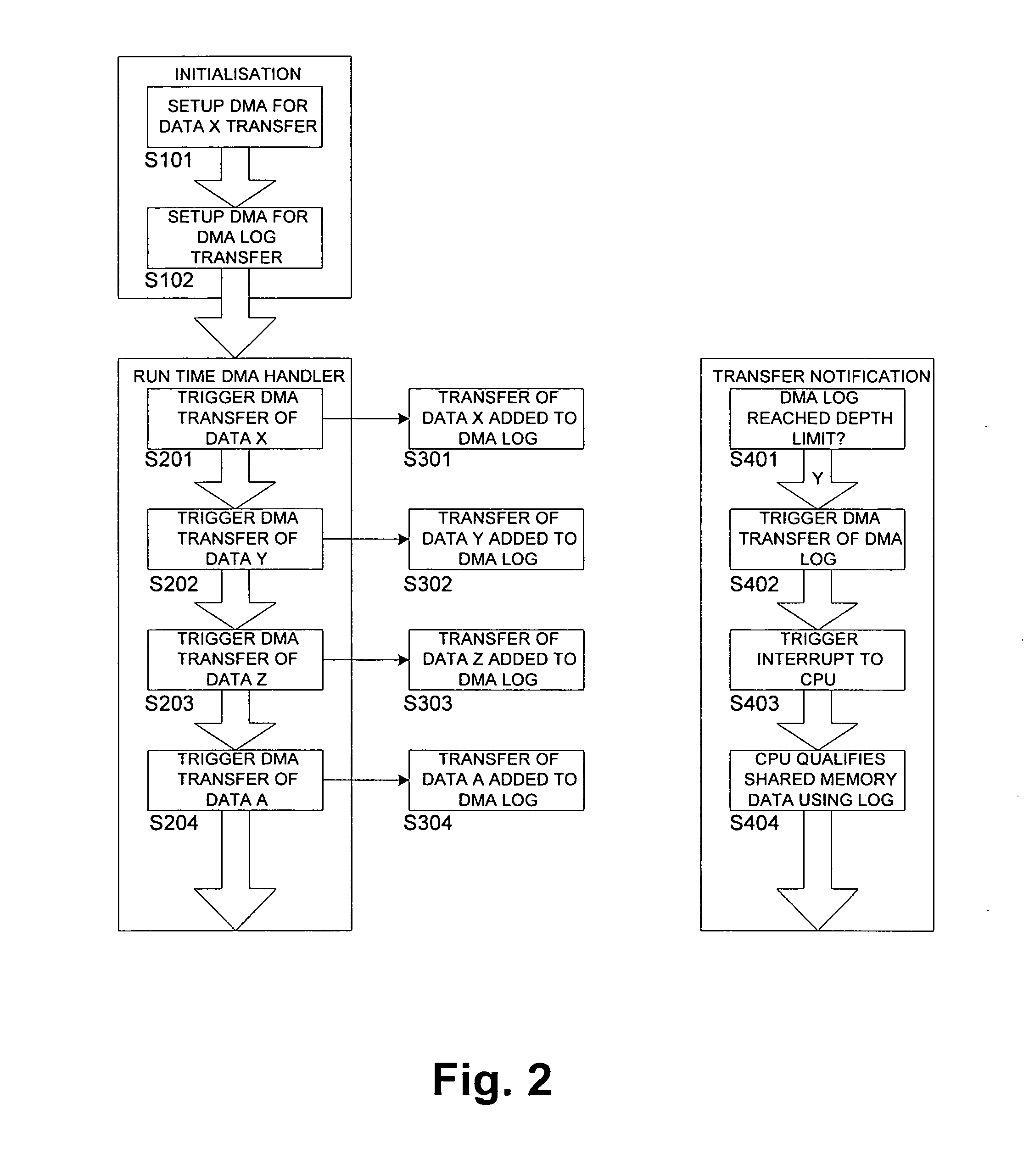
The present invention relates to a method and system for performing a data transfer between a shared memory (16) of a processor device (10) and a circuitry (20) connected to the processor device (10), wherein the data transfer is performed by triggering a DMA transfer of the data to the processor device, adding the DMA transfer to a transaction log, and providing the transaction log to the processor device, when the transaction log has reached a predetermined depth limit. The processor device is then informed of the DMA transfer of the transaction log, so as to be able to validate the transferred data. Thereby, significant background data movement can be provided without introducing high core overheads at the processor device (10).

Description

FIELD OF THE INVENTION [0001] The present invention relates to a method and system for performing a data transfer between a memory of a processor device, such as a digital signal processor (DSP), and a circuitry, such as an application specific integrated circuit (ASIC), connected to the processor device. BACKGROUND OF THE INVENTION [0002] Distributed memory architectures are very good at implementing data flow processing, and data flow processing is in turn what almost every DSP and related application boils down to. Ideal fit between DSP and data flow systems is further strengthened by the need for DSP application to run in real-time, i.e. they must process data with a specified throughput and / or latency requirement. Shared memory systems may have difficulties in guaranteeing latency due to the uncertainties over memory contention. [0003] If the central processing unit (CPU) of a DSP has to stop its current task and move data on and off the chip, performance will be poor. Therefor...

Claims


Application Information

Patent Timeline
IPC IPC(8): G06F13/28
CPCG06F13/28
Inventor BEALE, JOHN
Owner NOKIA SOLUTIONS & NETWORKS OY
Why Eureka
Eureka Blog
Learn More