Method of reducing the pattern effect in the CMP process
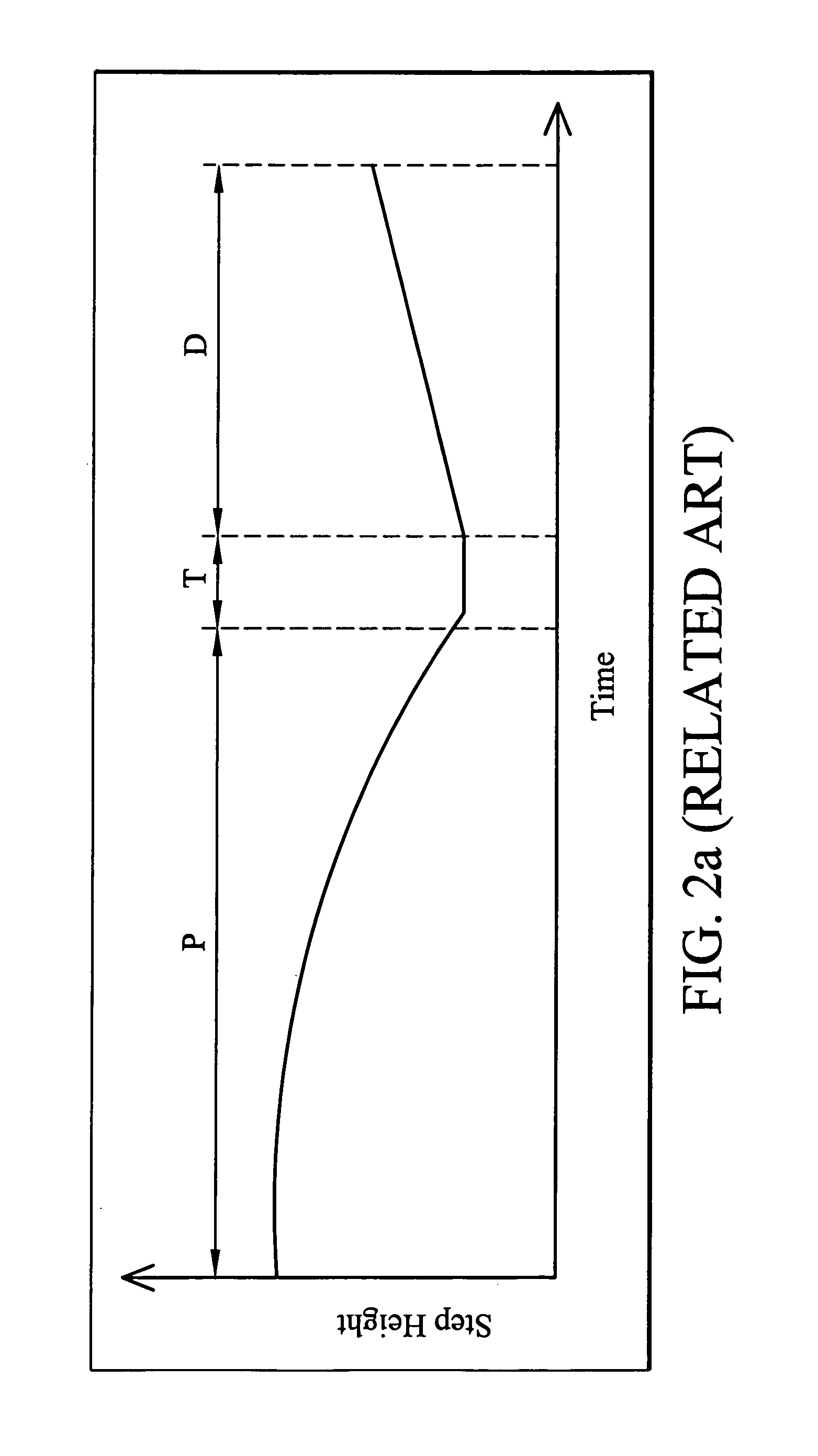
a technology of pattern effect and cmp, which is applied in the direction of semiconductor/solid-state device manufacturing, basic electric elements, electric apparatus, etc., can solve the problems of unsatisfactory pattern effect, dishing phenomenon, and deterioration of electrical properties, so as to reduce dishing phenomenon, improve the end-point detecting function of the polishing machine, and prolong the transition stage. the effect of tim
- Summary
- Abstract
- Description
- Claims
- Application Information
AI Technical Summary
Benefits of technology
Problems solved by technology
Method used
Image
Examples
example
Example 1
The Method of Reducing the Pattern Effect in the CMP Process According to the Present Invention
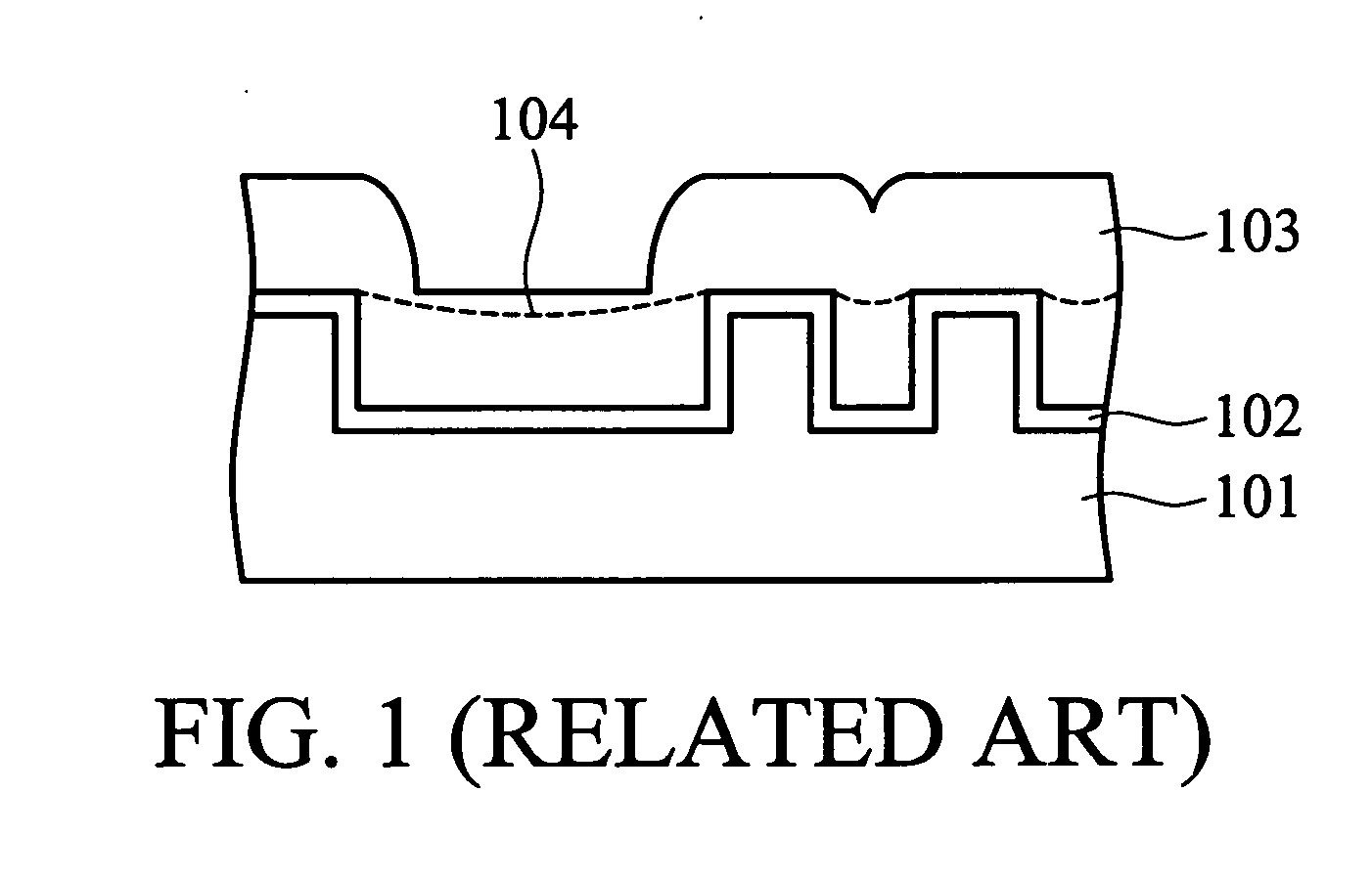
[0046] The example was performed using the method of reducing the pattern effect in the CMP process of the present invention mentioned above, wherein silicon dioxide was used as the patterned dielectric layer with trench patterns of squares (110×110 μm2) and isolated lines (5×350 μm2), TiN was used to form the barrier layer with a thickness of 250 ű50 Å, a copper layer was deposited as a conductive layer by copper seeding and then electrochemical plating on the TiN barrier layer and had a thickness of 6000 ű600 Å and average step heights of about 4900 Å for the square area and about 1500 Å for the isolated line area.
[0047] After the first CMP process was performed, the thickness of the remaining copper layer higher than the TiN barrier layer was about 4800 ű480 Šand was approximately planar. Copper was re-deposited on the remaining copper layer by electrochemical plating to...
example 2
The Method of Eliminating the Dishing Phenomena after a CMP Process According to the Present Invention
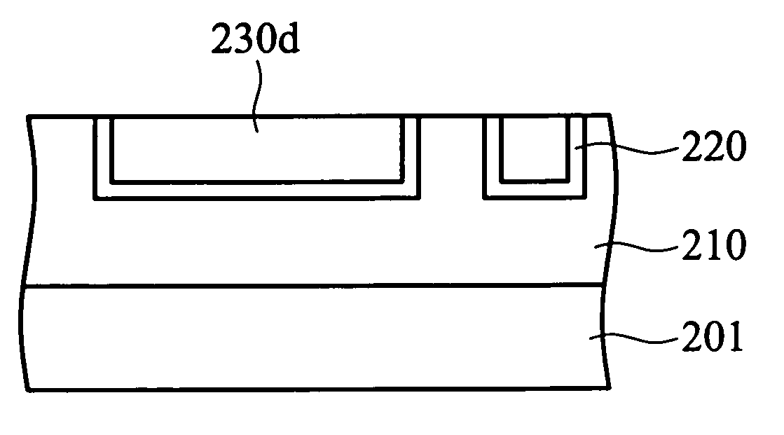
[0051] A semiconductor substrate with dishing phenomena after a CMP process was provided. The semiconductor substrate contained a patterned dielectric layer, a TiN barrier layer with a thickness of 250 ű50 Å, an end-point-polished copper layer with a dishing depth of about 1200 Å at the trench pattern. A layer of copper was electrochemically plated on the polished copper layer, resulting a copper layer with a total thickness (from the top surface of the barrier layer to the top surface of the copper layer) of about 6000 Å. Then, a CMP process was performed. At the end of the CMP process, a planar surface of the copper layer was obtained.
PUM
 Abstract
Description
Claims
Application Information


