Optical semiconductor package

a technology of optical semiconductors and semiconductor lasers, applied in the direction of semiconductor lasers, instruments, optical elements, etc., can solve the problems of high frequency transmission characteristics of packages, signal quality degradation, and high cost of ceramic substrates per unit area

Inactive Publication Date: 2005-06-09
MITSUBISHI ELECTRIC CORP
View PDF3 Cites 34 Cited by
  • Summary
  • Abstract
  • Description
  • Claims
  • Application Information

AI Technical Summary

Benefits of technology

[0014] An optical semiconductor package according to the present invention is an optical semiconductor package for packaging therein an optical semiconductor element, and includes a stem with a hole; a dielectric sealed into the hole of the dielectric, and wit

Problems solved by technology

Since they are single-phase can packages, impedance mismatching tends to occur in front and rear portions (portions in which the pins from the dielectric are exposed to an air layer) of a feed-through (a part in which the pins are covered with dielectric) when a modulated signal at 10 Gb/s or more is to be transmitted, and high frequency transmission characteristics of the package become worse.
In addition, a dummy resistor is disposed outside of the package, so that a signal quality degrades when a modulated signal is transmitted at 10 Gb/s or more.
The ceramic substrate itself per unit area is expensive.
In order to connect the multilayer ceramic feed-through to a lead,

Method used


Image

  • Optical semiconductor package
  • Optical semiconductor package
  • Optical semiconductor package

Examples


first embodiment

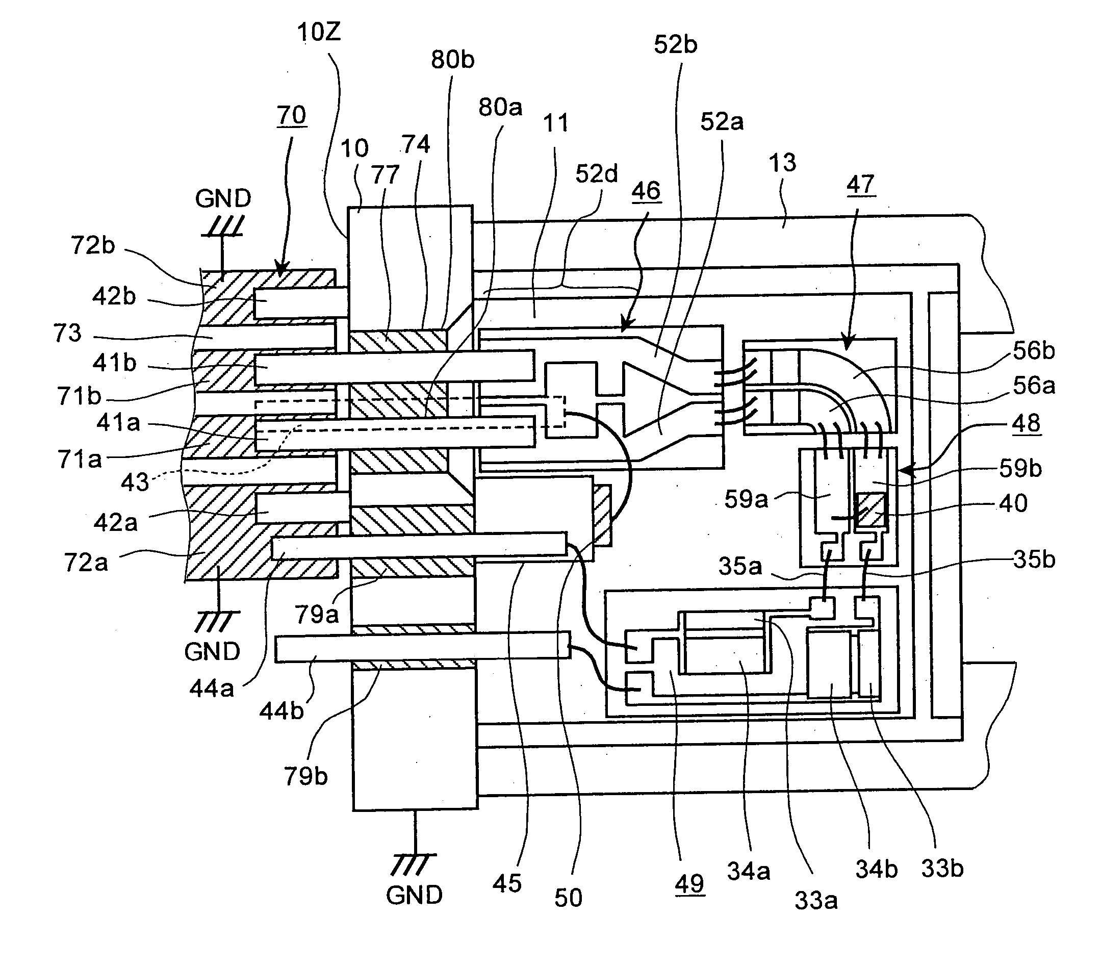
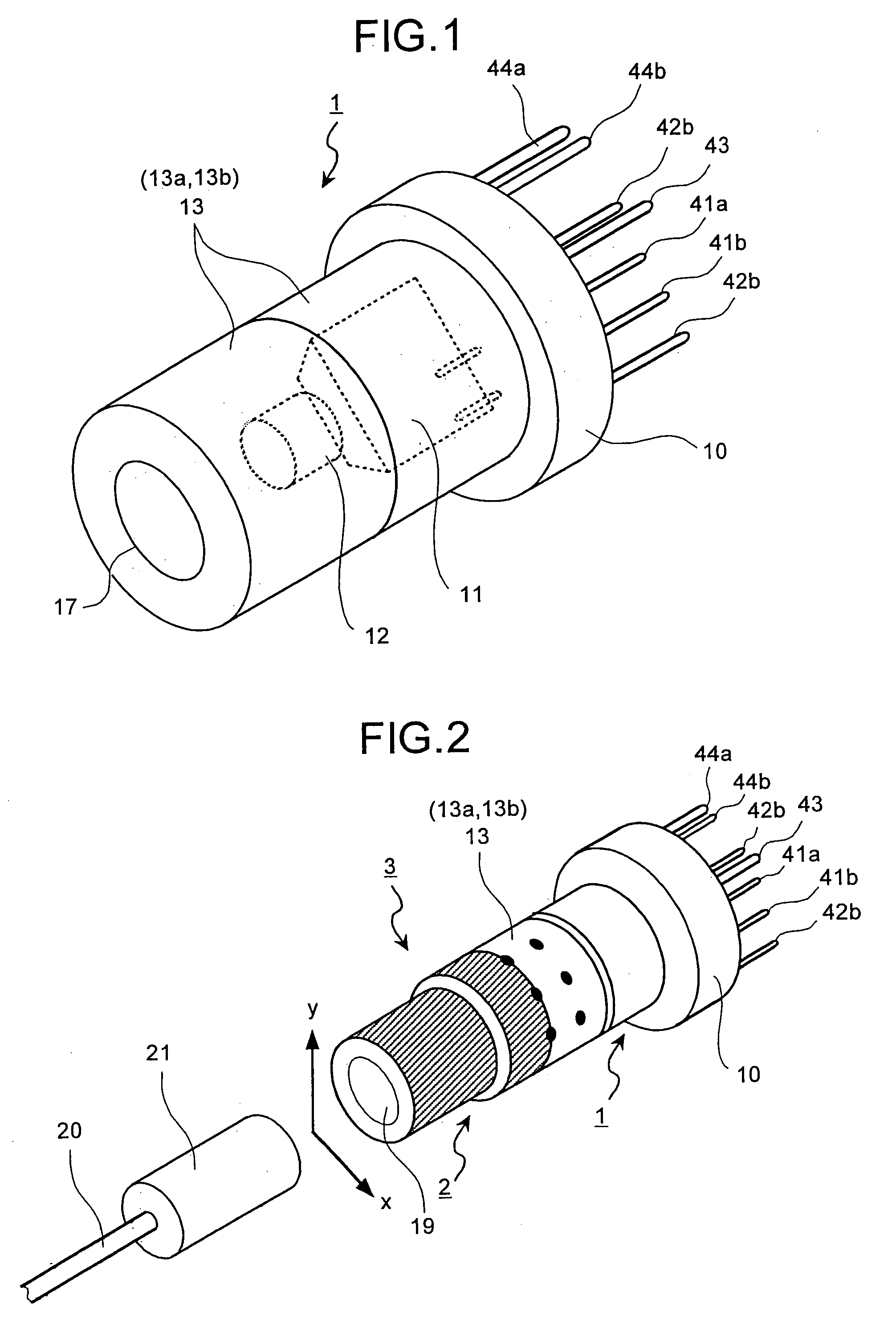
[0051] The optical semiconductor package employed in an optical semiconductor module in the first embodiment of the present invention will be explained with reference to FIG. 1 to FIG. 17. The optical semiconductor package in the first embodiment adopts an inexpensive can package type module form, and includes therein a laser diode (hereinafter, “LD”) serving as an optical semiconductor element. In this specification, it is assumed that the optical semiconductor package is a generic term embracing even a package without a sealing cap.

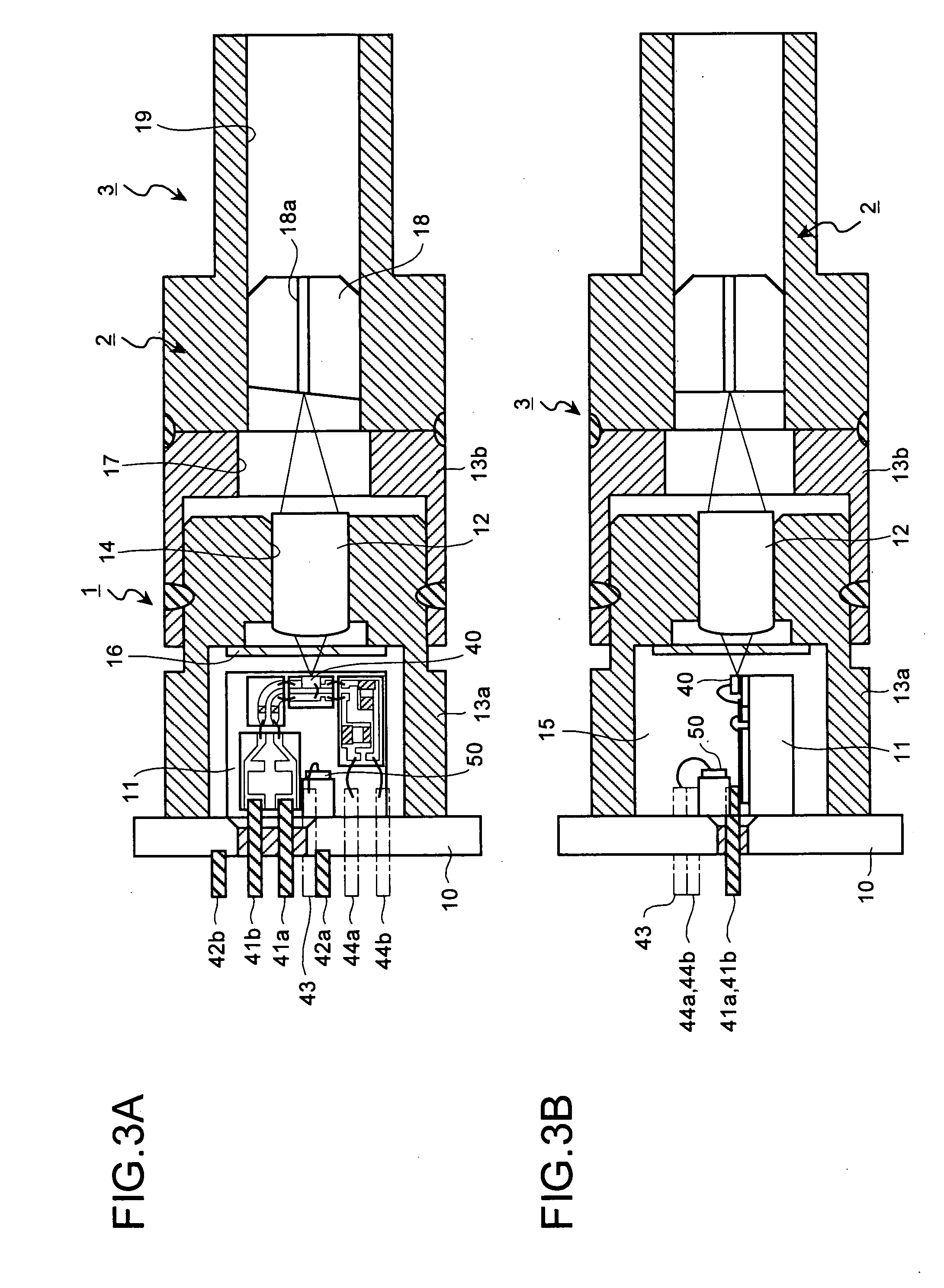
[0052]FIG. 1 is an outer perspective view of the optical semiconductor package (hereinafter, “can package”) 1. FIG. 2 is an outer perspective of the optical semiconductor element module 3 (hereinafter, “LD module” since an example of packaging an LD in the package will be mainly explained in this embodiment) including the can package 1 and a receptacle 2. FIG. 3A is a horizontal sectional view (a view in a direction parallel to an x axis shown in FIG. ...

second embodiment

[0144] The second embodiment of the present invention will be explained with reference to FIGS. 19A to 19C. FIG. 19A to FIG. 19B illustrate the other shapes of the dielectric 77 for sealing the high frequency signal pins 41a and 41b.

[0145] In FIG. 19A, the cocoon shape in which two circles are connected to each other by a straight line (or a gentle curve) is adopted as the shape of the dielectric. If attention is paid to distances from one pin 41a (or 41b) to peripheral edges of the dielectric 77, that is, to the stem 10 serving as a ground member, then distances of a part around about 270 degrees at the center of the pin 41a (or 41b) are equal, i.e., r, and the distances of the remaining parts from the pin 41a (or 41b) are larger than the distance r. If the dielectric is oval as employed in the first embodiment, then distances of a part around about 180 degrees at the center of the pin 41a (or 41b) are equal, i.e., r, and the distances of the remaining parts from the pin 41a (or 4...

third embodiment

[0147] The third embodiment of the present invention will be explained with reference to FIG. 20. In the third embodiment, the stem 10 is constituted to have a multi-structure so as to reduce the cost of the stem 10.

[0148] In the stem 10 in the third embodiment shown in FIG. 20, the high frequency signal pins 41a and 41b are arranged substantially in the central portion of the stem 10, and the oval dielectric 77 consisting of soda-barium glass is arranged around the high frequency signal pins 41a and 41b each consisting of Kovar. A first stem member 10a substantially equal in coefficient of thermal expansion to the dielectric 77 and consisting of Kovar is arranged so as to prevent cracks from occurring to the dielectric 77. A second stem member 10b consisting of an inexpensive material, such as iron, having a relatively good thermal conduction is arranged outside of the first stem member 10a. By arranging the members 10a and 10b, the radiation characteristics are improved. As a mat...


PUM


Abstract

Includes a stem with a hole, a dielectric sealed into the hole of the stem and including a pair of pin insertion holes, and a pair of high frequency signal pins that penetrate and fit into the pair of pin insertion holes of the dielectric, and constituting differential lines connected to an optical semiconductor element.

Description

TECHNICAL FIELD [0001] The present invention relates to an optical semiconductor package in which an optical semiconductor element such as a semiconductor laser is packaged, and more specifically relates to a coaxial module to which an optical fiber is attached or an optical semiconductor element module to which a receptacle adapter for connecting an optical fiber is attached. BACKGROUND ART [0002] In recent years, an optical signal transmission rate of an optical communication system that transmits an optical signal through an optical fiber has been rapidly accelerating so as to satisfy an increase in communication traffic as the Internet spreads. Likewise, a transmission rate of an optical transmitter-receiver has shifted from 2.5 Gb / s to 10 Gb / s, and research and development are underway with a view of realizing a transmission rate of 40 Gb / s. Accordingly, there an increasing needs to accelerate a transmission rate of a signal handled by an optical transmitter-receiver. [0003] Th...

Claims


Application Information

Patent Timeline
IPC IPC(8): G02B6/42H01S5/022
CPCG02B6/4201G02B6/4204G02B6/4206G02B6/421G02B6/4292H01S5/06226H01S5/02216H01S5/02248H01S5/02284H01S5/0427H01S5/02212G02B6/4279H01L2224/48091H01S5/02251H01S5/02325H01L2924/00014
Inventor ARUGA, HIROSHITAKAGI, SHINICHISAKAI, KIYOHIDE
Owner MITSUBISHI ELECTRIC CORP
Why Eureka
Try Eureka