

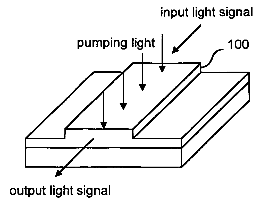
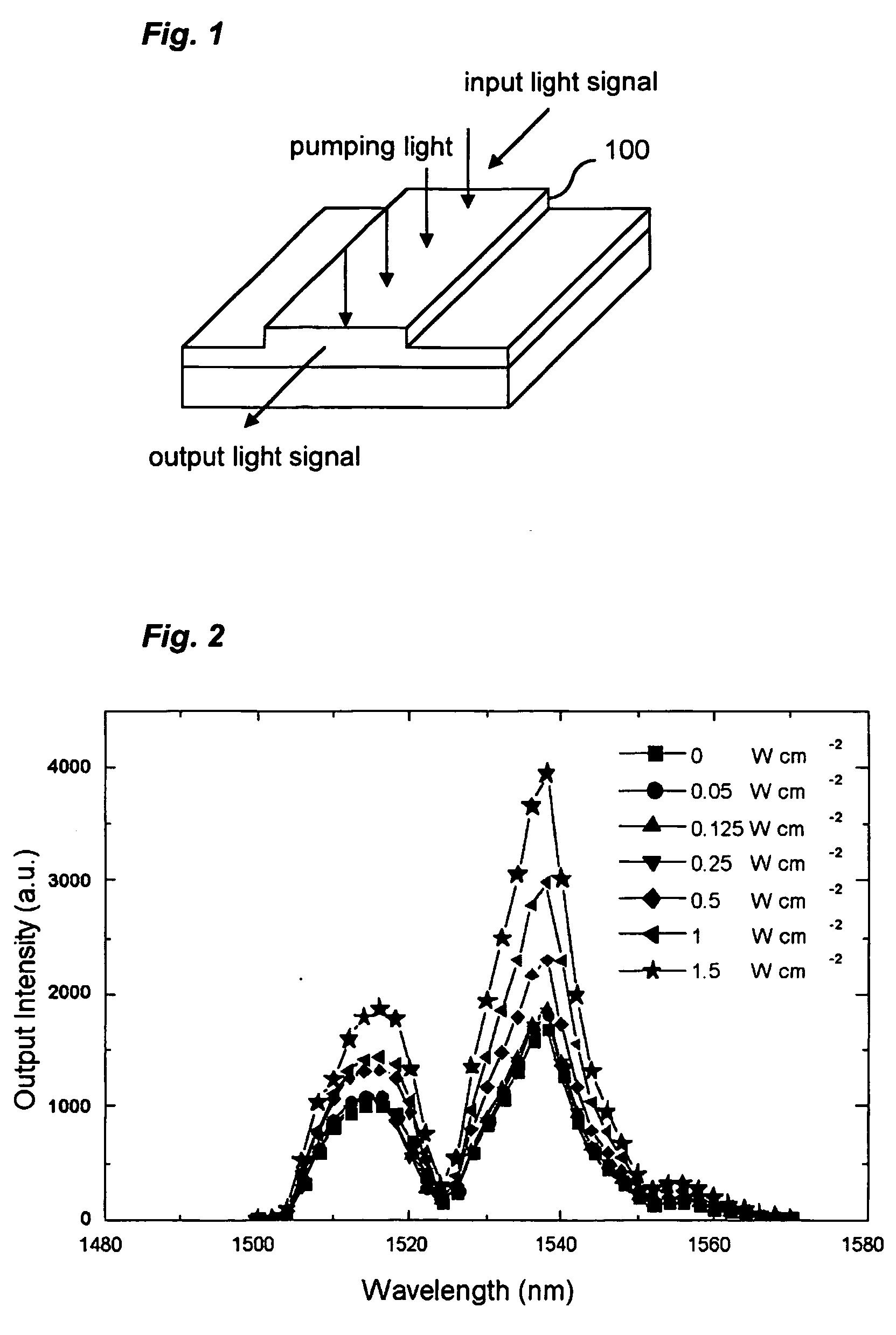
Top-pumped waveguide amplifier
a waveguide amplifier and top-pumped technology, applied in the direction of instruments, cladded optical fibres, active medium materials, etc., can solve the problems of reducing the actual pump power, unable to allow all light from the light source to enter the waveguide, and lowering the excitation efficiency, so as to achieve efficient focus
- Summary
- Abstract
- Description
- Claims
- Application Information
AI Technical Summary
Benefits of technology
Problems solved by technology
Method used
Image

Examples
first embodiment
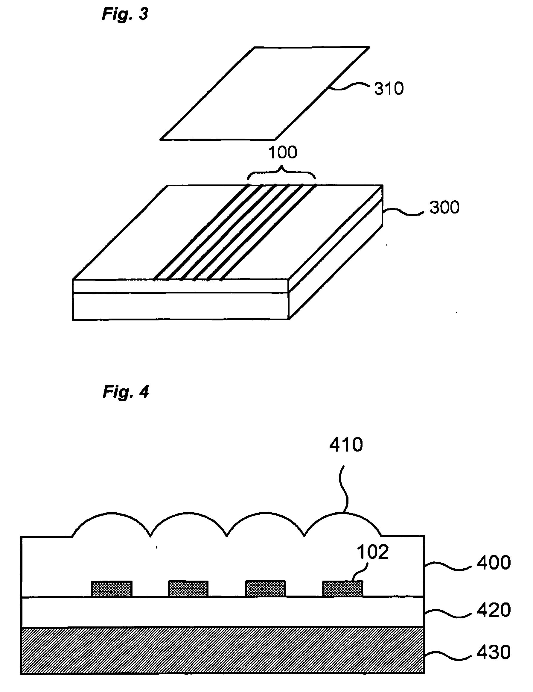
[0029] It is understood that in order to increase the pumping efficiency, after collecting light from a light source using an optical device such as a lens, a waveguide can be pumped using the light so collected. However, because the size of the waveguide is very small and costly, there is a limitation to the use of such a separate optical device. Therefore, in order to collect light at a low price, prominences 410 are formed on an upper cladding layer 400 of core layers 102 to act as convex lenses, as shown in FIG. 4. The prominences 410 are formed in a linear arrangement, similar to the core layers 102. They may be formed by etching the upper cladding layer 400, or by using a polymer such as PMMA subsequent to vapor deposition of the upper cladding layer 400.
[0030] In case of etching the upper cladding layer 400 for the purpose of forming the prominences 400, a “diffusion-limited etching process” can be used. Although such an etching process is little used in manufacturing of sem...
second embodiment
[0032]FIG. 5 is a schematic cross sectional view showing a waveguide amplifier using the optical focusing technique according to the second embodiment of the present invention. According to the second embodiment of the present invention, a pump light is focused onto a core layer 102 using the reflection of a concave mirror M1 which is formed by deeply etching and then coating a lower cladding layer 422. In this case, the position of the core layer 102 and the curvature of the concave mirror M1 are modulated in order for the core layer 102 to be positioned at the focal point of the concave mirror M1. In FIG. 5, reference number 412 indicates an upper cladding layer.
third embodiment
[0033] In the second embodiment, a deep etching process was used to form a mirror surface. In the case that it is somewhat difficult to carry out such a process, it is preferable to use a mirror without a deeply etched structure. FIG. 6 is a schematic cross sectional view showing a waveguide amplifier using the optical focusing technique according to the third embodiment of the present invention. Reference is made to FIG. 6, first, grooves in the form of line are formed in a transparent substrate 432. Then, the grooves are mirror coated to thereby form mirrors M2. Similar to the second embodiment, the core layer 102 is positioned at the focal point of each mirror M2.
Industrial Applicability
[0034] As apparent from the above description, the present invention provides a waveguide amplifier with low cost and high efficiency, resulting from increasing the pump light efficiency per waveguide using a wide band light source. This enables integration of optical devices as well as lowering...
PUM
 Abstract
Description
Claims
Application Information