Exposure apparatus

a technology of exposure apparatus and scanning light, which is applied in the field of exposure apparatus, can solve the problems of inability to measure or correct the tile of the image surface in the scan direction, the depth of focus (“dof”) is excessively small, and the short wavelength of the exposure light cannot meet the rapid progressing integration, etc., and achieves superior resolution and high precision focus calibration. the effect of lowering the throughpu

Active Publication Date: 2005-06-16
CANON KK
View PDF3 Cites 43 Cited by
  • Summary
  • Abstract
  • Description
  • Claims
  • Application Information

AI Technical Summary

Benefits of technology

[0016] Accordingly, it is an exemplary object of the present invention to provide an exposure apparatus that realizes a highly precise focus calibration by measuring a tilt of an image surface in a scan direction, and provides exposure with a superior resolution without lowering a throughput.

Problems solved by technology

However, only the short wavelength of the exposure light cannot satisfy the rapidly progressing integration of the semiconductor devices.
This configuration, however, makes a depth of focus (“DOF”) excessively small, and demands for the remarkably improved detecting accuracy of the focal point, in particular, improved accuracy of the focus calibration.
It is possible to measure and correct the tilt of the image surface in the long side direction, as described above, in the conventional scanning exposure apparatus, but it is not possible to measure or correct the tile of the image surface in the scan direction.
However, when the stage running surface does not accord with the tilt of the image surface of the projection optical system, the reference surface correction of the focus / leveling detecting system deteriorates.

Method used


Image

  • Exposure apparatus
  • Exposure apparatus
  • Exposure apparatus

Examples


Embodiment Construction

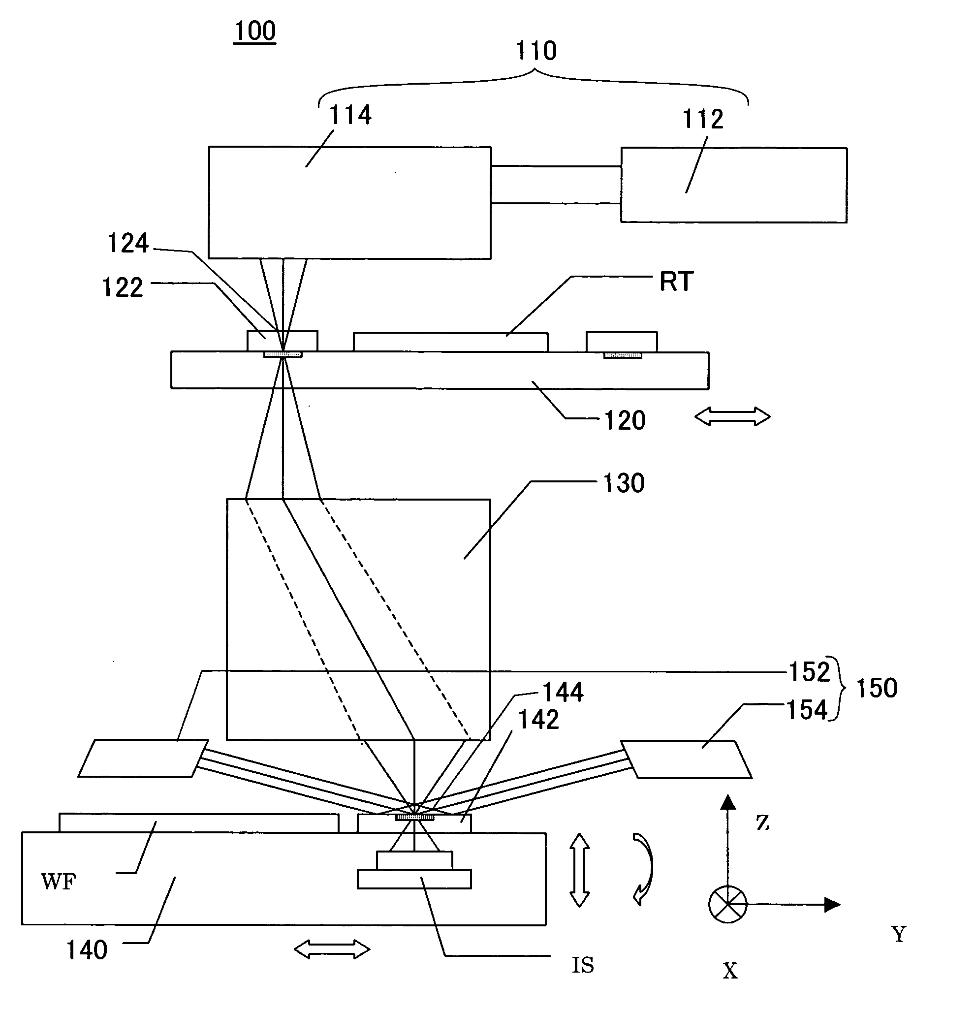
[0033] Referring now to the accompanying drawings, a description will be given of an exposure apparatus according to one aspect of the present invention. A like element in each figure is designated by the same reference numeral, and a duplicate description thereof will be omitted. Here, FIG. 1 is a schematic block diagram of the exposure apparatus 100 according to one aspect of the present invention.

[0034] The exposure apparatus 100 is a scanning exposure apparatus that exposes a circuit pattern on a reticle RT onto a wafer WF in a step and scan manner. This exposure apparatus is suitable for a sub-micron or quarter-micron lithography process. The exposure apparatus 100 includes, as shown in FIG. 1, an illumination apparatus 110, a reticle stage 120, a projection optical system 130, a wafer stage 140, and a focus / leveling detecting system 150.

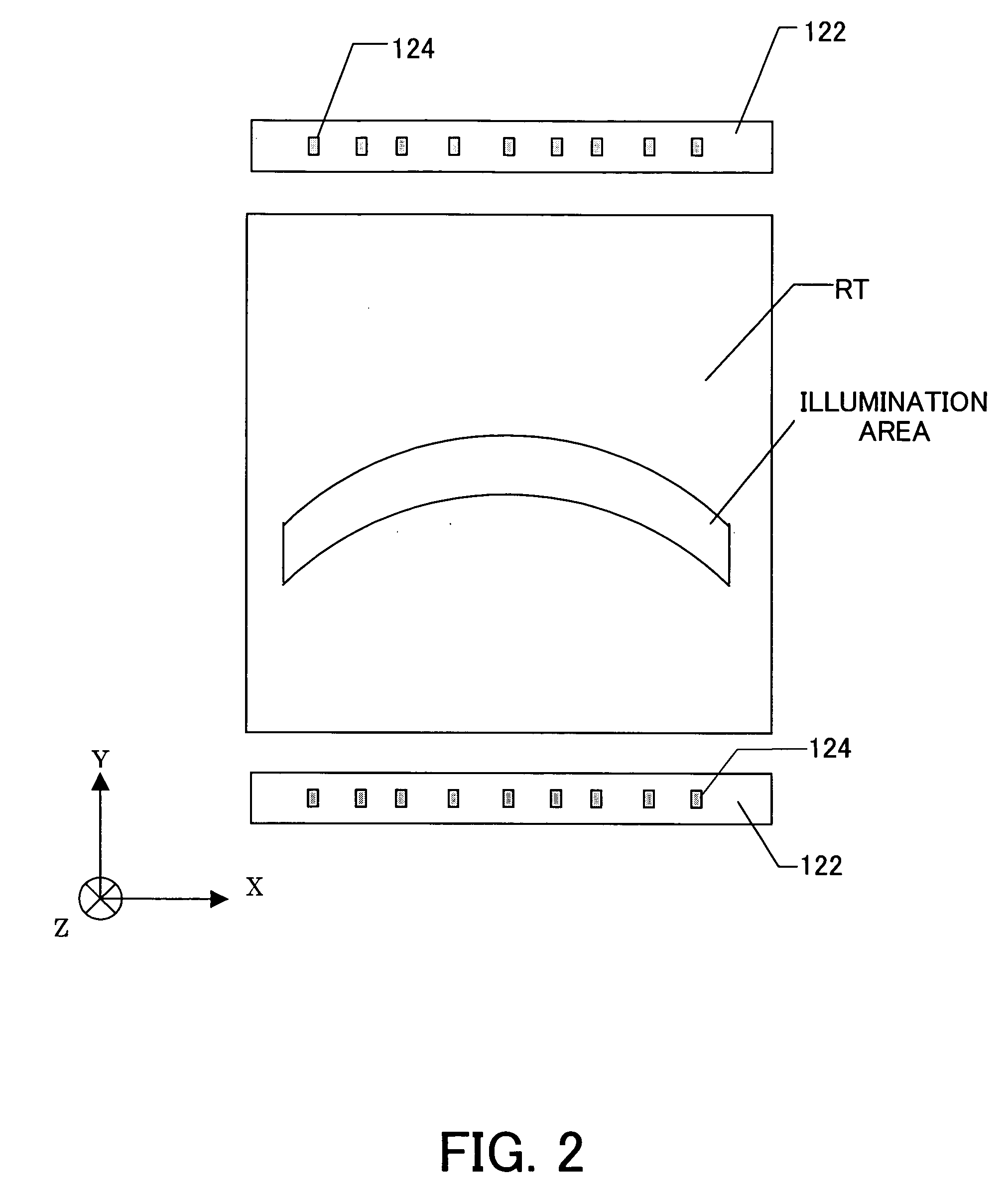
[0035] The illumination apparatus 110 illuminates the reticle RT on which a circuit pattern to be transferred is formed, and includes a ligh...


PUM

PropertyMeasurementUnit
wavelengthaaaaaaaaaa

Abstract

An exposure apparatus includes a projection optical system for projecting a pattern on a reticle mounted on a first stage onto an object mounted on a second stage, a first reference plate provided on the reticle or a surface equivalent to the reticle, the first reference plate having three or more first reference marks each of which serves as a reference for an alignment between the reticle and the object, a measuring unit for measuring focus position at imaging positions of the first reference marks and for measuring an image surface of the projection optical system, and a correcting unit for correcting a relationship between the image surface and a reference surface as a reference of a measurement by the measuring unit.

Description

BACKGROUND OF THE INVENTION [0001] The present invention relates generally to an exposure apparatus, and more particularly to an exposure apparatus used to manufacture various devices including semiconductor chips such as ICs and LSIs, display devices such as liquid crystal panels, sensing devices such as magnetic heads, and image pickup devices such as CCDs, as well as fine patterns used for micromechanics. The present invention is suitable, for example, for a step-and-scan exposure apparatus in the lithography process. [0002] Conventionally employed reduction projection exposure apparatuses use a projection optical system to project or transfer a circuit pattern on a mask or a reticle onto a wafer, etc., in manufacturing such a fine semiconductor device as a semiconductor memory and a logic circuit in the photolithography technology. [0003] Recently, as shown in FIG. 13, in order to improve the resolution and enlarge the exposure apparatus, a scanning projection exposure apparatus...

Claims


Application Information

Patent Timeline
Patent Type & Authority Applications(United States)
IPC IPC(8): G01B11/26G01B11/00G03F7/20G03F9/00H01L21/027
CPCG03F9/7034G03F9/7026
Inventor MIURA, SEIYA
Owner CANON KK
Why Eureka
Try Eureka