Method for cleaning a plasma enhanced CVD chamber

Active Publication Date: 2005-06-23
TAIWAN SEMICON MFG CO LTD
View PDF5 Cites 37 Cited by
  • Summary
  • Abstract
  • Description
  • Claims
  • Application Information

AI Technical Summary

Problems solved by technology

One problem with PECVD and HDP-CVD processes is the formation of coatings of IMD layer deposition material over surfaces within the plasma reactor.
The formation of residual deposition material becomes a problem in subsequent CVD depositions in several respects including flaking off of the residual deposition material onto the process wafer during a PECVD deposition process thereby introducing defects into a newly deposited CVD layer, for example an IMD layer.
In addition, the presence of dopants, such as fluorine in prior art processes has tended to cause problems in subsequent depositions of non-doped IMD layers by undesirably introducing fluorine contaminants due to interaction of the deposition plasma with the residual deposition material within the chamber.
However, the down time of the plasma reactor chamber and the labor intensive requirements for manual preventative maintenance functions increases the cost of manufacture proportionate to the frequency of such required maintenance.
Unfortunately this approach makes the cleaning processes more difficult as the protective coatings are generally more resistant to cleaning processes, including plasma cleaning processes, requiring the use of fl

Method used


Image

  • Method for cleaning a plasma enhanced CVD chamber
  • Method for cleaning a plasma enhanced CVD chamber

Examples


Embodiment Construction

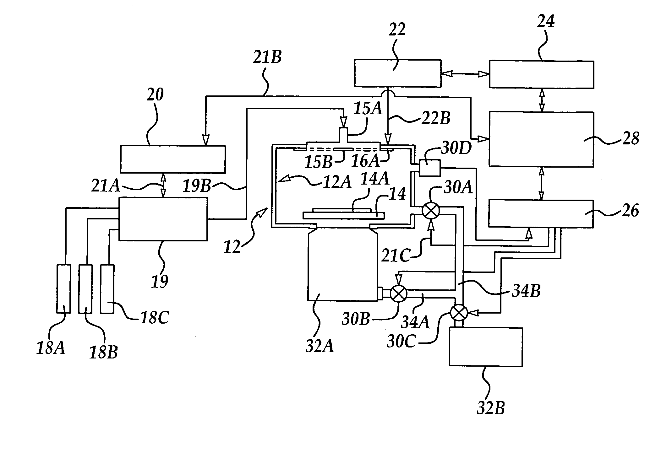
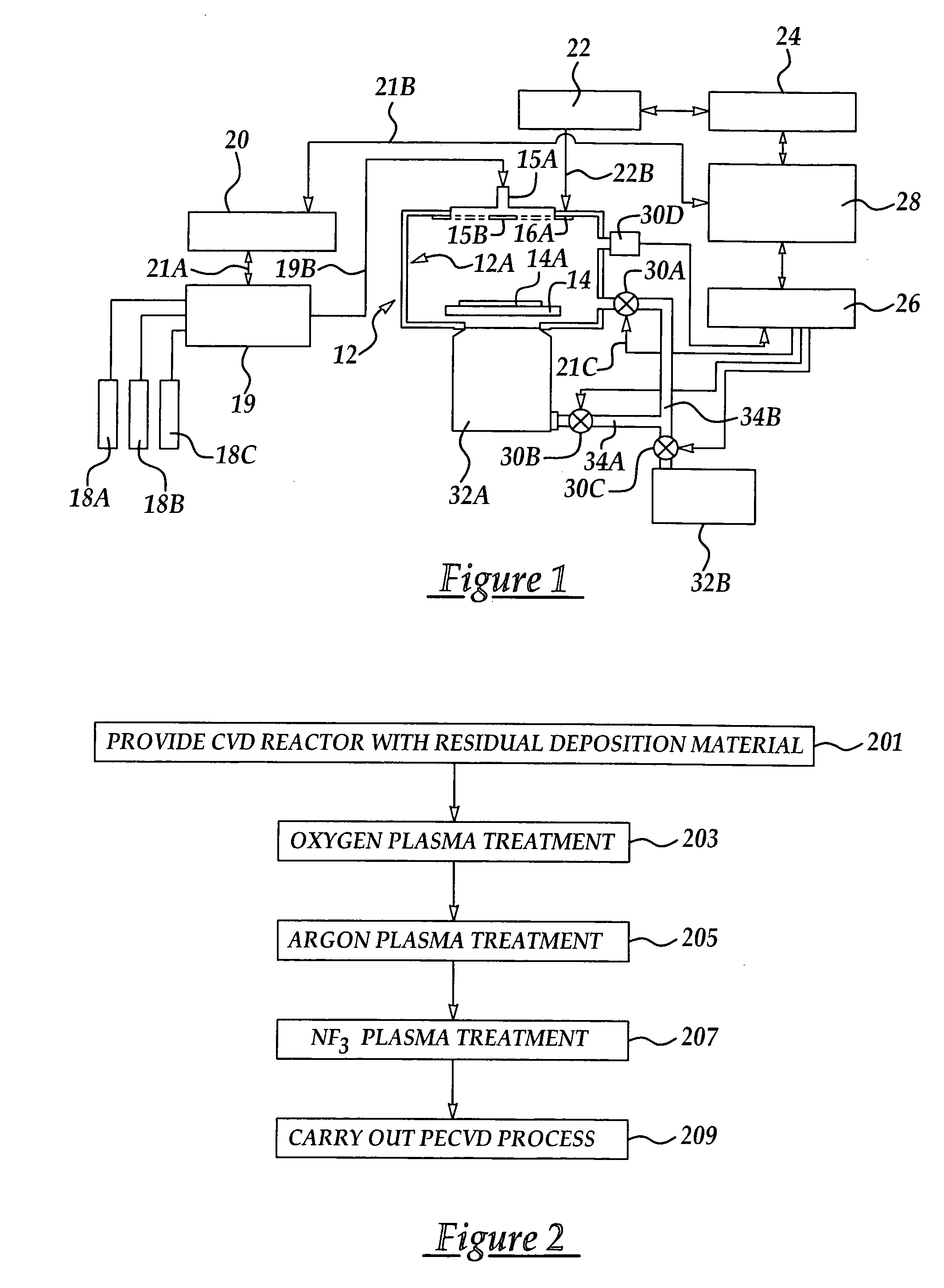
[0016] Although the present invention is explained by reference to an exemplary CVD plasma reactor, it will be that the method of the present invention applies generally to CVD plasma reactors whereby the improved plasma cleaning process according to embodiments of the present invention are used to reduce the usage of fluorine containing gases in the cleaning process including eliminating the use of fluorocarbons, while improving a plasma cleaning operation to reduce particulate contamination and improve a subsequent deposited CVD film uniformity.

[0017] Referring to FIG. 1 is shown an exemplary PECVD reactor to illustrate embodiments of the plasma cleaning process according to embodiments of the present invention. Shown is a plasma reactor chamber 12 including wall portions e.g., 12A where a film of residual deposition material forms following a conventional PECVD deposition process. It will be appreciated that the film of residual deposition material may form over all exposed surf...


PUM

PropertyMeasurementUnit
Percent by volumeaaaaaaaaaa
Chemically inertaaaaaaaaaa

Abstract

A method for plasma cleaning a CVD reactor chamber including providing a plasma enhanced CVD reactor chamber comprising residual deposited material; performing a first plasma process comprising an oxygen containing plasma; performing a second plasma process comprising an argon containing plasma; and, performing a third plasma process comprising a fluorine containing plasma.

Description

FIELD OF THE INVENTION [0001] This invention generally relates to semiconductor device manufacturing methods and more particularly to a method for plasma cleaning a plasma enhanced CVD reactor chamber to improve CVD film deposition uniformity while reducing manufacturing and environmental costs. BACKGROUND OF THE INVENTION [0002] In forming multi-level integrated circuit devices, a major portion of the manufacturing cycle involves chemical vapor deposition (CVD), for example plasma enhanced CVD (PECVD) and high density plasma CVD (HDP-CVD), to deposit material layers. In particular, the depositing of oxide insulating layers, also preferred to as inter-metal dielectric (IMD) layers is performed several times in the formation of a multi-level integrated circuit device. [0003] Generally, the formation of IC devices involves a major effort in forming multiple levels of wiring, also referred to as damascene structures, which are formed by backfilling metals, for example copper, into open...

Claims


Application Information

Patent Timeline
IPC IPC(8): B08B6/00B08B7/00C23C16/44H01L21/00H01L21/30H01L21/3065
CPCB08B7/00C23C16/4405Y10S438/905Y10S134/902H01L21/67069
Inventor CHEN, SHENG-WENJANGJIAN, SHIU-KOCHANG, HUNG-JUIWANG, YING-LANG
Owner TAIWAN SEMICON MFG CO LTD
Why Eureka
Try Eureka