Semiconductor integrated circuit, semiconductor device, and manufacturing method of the semiconductor integrated circuit

a semiconductor integrated circuit and integrated circuit technology, applied in the direction of semiconductor devices, electrical devices, transistors, etc., can solve the problems of inability to easily form rewritable nonvolatile memory on glass substrates, inability to rewritable nonvolatile memory easily, and inability to meet the requirements of the product and the product surface, so as to improve the efficiency of material utilization and reduce the cost. , the effect of suppressing the increase in the cos

Inactive Publication Date: 2005-06-23
SEMICON ENERGY LAB CO LTD
View PDF33 Cites 93 Cited by
  • Summary
  • Abstract
  • Description
  • Claims
  • Application Information

AI Technical Summary

Benefits of technology

[0019] According to the invention, a photomask is not required to be thrown away after use and the increase in the cost can be suppressed as compared with in the case of all the data in ROMs being determined by a photomask. In addition, a metal wiring is drawn by a droplet discharging method, resulting in improved efficiency of material utilization, cost reduction, and a smaller amount of waste liquid to be treated. As a result, the cost of equipment investment and the production time can be reduced, resulting in the cost reduction of an ID chip.
[0020] As a result, an ID chip with increased impact resistance can be provided at low cost.
[0021] The ID chip of the invention is formed on a glass substrate or the like, therefore, the cost thereof can be reduced as compared with the one using a conventional silicon wafer. As for an integrated circuit with extremely low unit price such as an ID chip, the cost reduction leads to great profits.
[0022] According to the invention, the ink jet method or the laser cutting method of a metal wiring is adopted for the step of determining ROM data. Therefore, a photomask is not required to be thrown away after use in the step of determining ROM data, resulting in an ID chip with lower cost.
[0023] Further, depending on the application of the ID chip, a semiconductor integrated circuit formed on a glass substrate is transposed to a flexible substrate, resulting in an ID chip with increased impact resistance.
[0024] Moreover, according to the invention, information exchange or information management can be performed more simply and in a shorter time, and various information can be provided as compared with an information providing means such as a bar code. In addition, a semiconductor integrated circuit included in the ID chip of the invention is much thinner than a conventional one using a silicon wafer, thus an attractive design thereof can be maintained even when it is attached to a container of goods.

Problems solved by technology

In addition, since a chip formed on a silicon substrate is thick, irregularity occurs on the surface of products and goods, in particular when the chip is mounted on papers such as bills or on labels attached to the products and goods.
As a result, the design of the products and goods becomes less attractive.
Further, a rewritable nonvolatile memory is not easily formed on a glass substrate because of the restriction on the process temperature and the like.
However, stored data is necessarily different in each chip, thus in the case of a mask ROM being used, a photomask used in the step for determining data content is thrown away after use, leading to the increase in the cost of the chip.
Since the unit price of such a chip is extremely low, increased cost prohibits the spread thereof.

Method used


Image

  • Semiconductor integrated circuit, semiconductor device, and manufacturing method of the semiconductor integrated circuit
  • Semiconductor integrated circuit, semiconductor device, and manufacturing method of the semiconductor integrated circuit
  • Semiconductor integrated circuit, semiconductor device, and manufacturing method of the semiconductor integrated circuit

Examples


embodiment 1

[0068] Described in this embodiment is a memory cell example that configures a ROM using a precharge method.

[0069]FIG. 5A is a circuit diagram of a memory cell of a ROM using the precharge method. Each TFT in the memory cell is connected to a bit line 501 and a word line 504. One of two high density impurity regions of a TFT may be or not be connected to a GND 503 depending on data content.

[0070] For example, data is 0 in the case of a read potential being GND while data is 1 in the case of a read potential being VDD. In the case of a ROM adopting the precharge method, one of the two high density impurity regions of a TFT in a memory cell is connected to the GND or brought into a floating state. Therefore, a VDD wiring is not required in a memory cell array, resulting in reduction in the memory cell area.

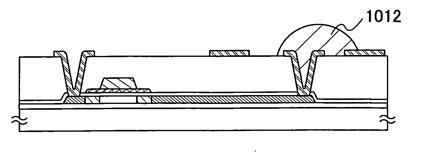
[0071]FIG. 5B is an example of a memory cell layout in the case of data content of a ROM adopting the precharge method being determined by the ink jet method. A memory cell inclu...

embodiment 2

[0075] Described in this embodiment is a configuration example of a systemized ID chip.

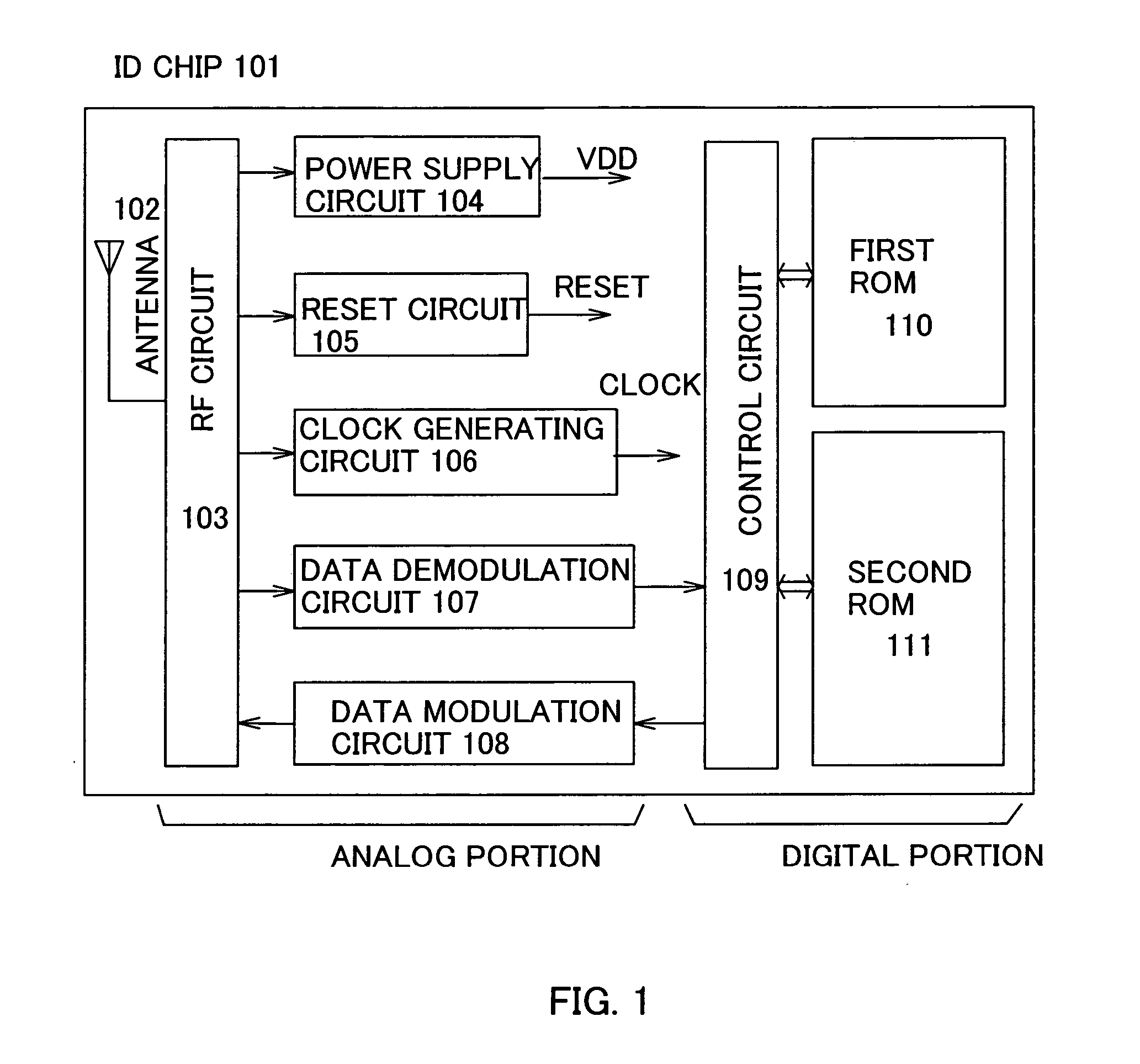
[0076] The invention can be applied to a high performance ID chip including a logic circuit such as a CPU. FIG. 6 shows a configuration example of such an ID chip. In FIG. 6, an ID chip 601 includes an antenna 602, an RF circuit 603, a power source circuit 604, a reset circuit 605, a clock generator circuit 606, a data demodulation circuit 607, a data modulation circuit 608, a control circuit 609, a CPU 610, a program ROM 611, a work RAM 612, a first ROM 613, and a second ROM 614.

[0077] The semiconductor integrated circuit shown in FIG. 6 is formed on a glass substrate or a flexible substrate. The antenna 602 may also be formed on the glass substrate or the flexible substrate, or may be formed outside the substrate and connected to the semiconductor integrated circuit inside the substrate.

[0078] Since the ID chip shown in FIG. 6 includes the CPU 610, it can incorporate various functions in addi...

embodiment 3

[0081] Described in this embodiment is a specific example of data common to substrates (first data) and data different between substrates (second data) according to the invention.

[0082]FIG. 7A shows an example of a glass substrate 701 that includes 2m+n ID chips 702 arranged in 2m columns and 2n rows (m and n are positive integers). Each of the ID chips 702 is sequentially assigned a number of 702 (1), 702 (2), . . . , 702 (2m+n).

[0083] Each of the ID chips includes L-bit identification serial data as shown in FIG. 7B. The lower m+n bits represent first data common to substrates, which is stored in a first ROM whose data content is determined by a step using a photomask. The upper L−(m+n) bits represent second data different between substrates, which is stored in a second ROM whose data content is determined by the ink jet method or the laser cutting method.

[0084]FIG. 7C shows first data content of the lower bits. The data common to substrates has to be different between chips in...


PUM


Abstract

A chip with increased impact resistance, attractive design and reduced cost, and a manufacturing method thereof are provided. A semiconductor integrated circuit is formed on a large glass substrate, and a part of data of a ROM included therein is determined by an ink jet method or a laser cutting method. Accordingly, the cost can be reduced without requiring a photomask, resulting in an inexpensive ID chip. Further, depending on the application, the semiconductor integrated circuit is transposed to a flexible substrate, thereby an ID chip with improved impact resistance and more attractive design can be achieved.

Description

BACKGROUND OF THE INVENTION [0001] 1. Field of the Invention [0002] The present invention relates to a semiconductor integrated circuit formed on a glass substrate or a flexible substrate, a semiconductor device including the semiconductor integrated circuit, and a manufacturing method of the semiconductor integrated circuit. [0003] 2. Description of the Related Art [0004] In recent years, there has been a great need for an IC card or an IC tag capable of contactless data communication in all fields that require automatic identification, such as securities and goods management. Such an IC card or an IC tag is required to be small for increased impact resistance, inexpensive for disposable application, an affinity for paper in view of the management of securities in particular, and a large capacity memory in accordance with the increased amount of data. Thus, the development of an IC chip on a silicon substrate has been advanced by using various technologies to meet such requirements...

Claims


Application Information

Patent Timeline
Patent Type & Authority Applications(United States)
IPC IPC(8): H01L21/82H01L21/768H01L21/77H01L21/8246H01L27/02H01L27/105H01L27/112H01L27/12H01L27/13H01L29/786H01L31/036
CPCH01L21/76892H01L21/76894H01L2924/0002H01L21/76895H01L27/0207H01L27/105H01L27/112H01L27/11253H01L27/11293H01L27/12H01L27/1266H01L27/13H01L29/78624H01L27/1285H01L27/1292H01L2924/00H10B20/38H10B20/65H10B20/00H01L27/1214
Inventor KATO, KIYOSHI
Owner SEMICON ENERGY LAB CO LTD
Why Eureka
Try Eureka