Shift register and driving method thereof

a technology of shift register and driving method, which is applied in the direction of digital storage, multiple input and output pulse circuits, instruments, etc., can solve the problems of increasing layout area and power consumption, increasing power consumption, and difficulty in high frequency operation, and achieves low power consumption

Inactive Publication Date: 2005-06-23
SEMICON ENERGY LAB CO LTD
View PDF9 Cites 13 Cited by
  • Summary
  • Abstract
  • Description
  • Claims
  • Application Information

AI Technical Summary

Benefits of technology

[0009] Furthermore, a level shifter which amplifies a CK signal operates only in a short period where the amplification of a CK signal is required since the level shifter is operated by a control signal generated by using an output pulse of the shift register. Accordingly, shoot-through current flows only for a short time in the level shifter which amplifies a CK signal, which can provide a shift register of low power consumption.

Problems solved by technology

In the case of amplifying the CK signal by the external circuit, problems arise in that the number of components such as a level shifter IC and a power supply IC is increased, which consumes more power.
In the internal circuit, by providing an input portion of an FPC with a level shifter for amplifying the CK signal to supply it to all the stages of the shift register, problems arise in that the size of layout area and the power consumption are increased and a high frequency operation becomes difficult.
The shift register provided with the data transfer portion as a differential amplifier may not operate accurately in the case where the characteristics of transistors configuring the differential amplifier are not the estimated ones.
In a polysilicon TFT other than a single crystalline TFT, variation in characteristics is a considerable problem.

Method used


Image

  • Shift register and driving method thereof
  • Shift register and driving method thereof
  • Shift register and driving method thereof

Examples


embodiment mode 1

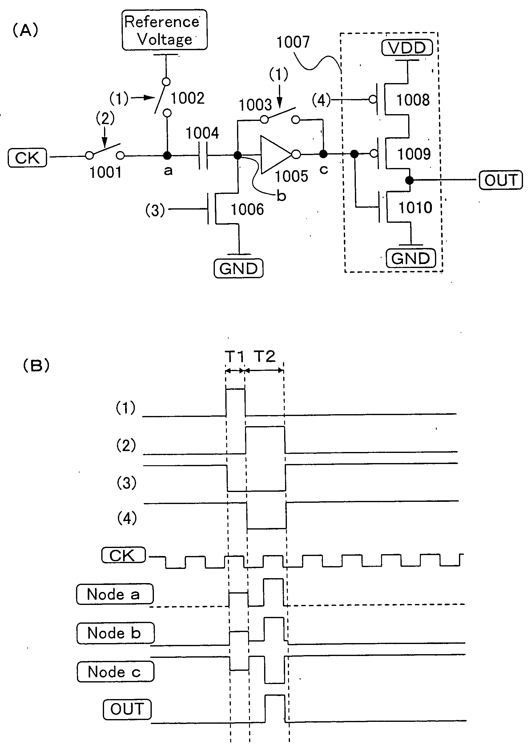
[0083]FIG. 1A shows a first structure of a level shifter which amplifies a CK signal of the shift register of the invention.

[0084] The level shifter of Embodiment Mode 1 includes a switch 1001 for receiving a CK signal, a reference switch 1002, a switch 1003 for setting a threshold value, a capacitor means 1004, a correction inverter 1005, a switch 1006 for fixing a potential, and an output inverter 1007. The output inverter 1007 includes a first P-type TFT 1008, a second P-type TFT 1009, and an N-type TFT 1010. The switch 1001 for receiving a CK signal is controlled to be turned ON / OFF by a signal (2) generated from an output pulse of the shift register to supply a CK signal. The reference switch 1002 is controlled to be turned ON / OFF by a signal (1) generated from an output pulse of the shift register to supply a reference voltage to a connection of the switch for receiving CK 1001 and the capacitor means 1004. The input portion and the output portion of the correction inverter 1...

embodiment mode 2

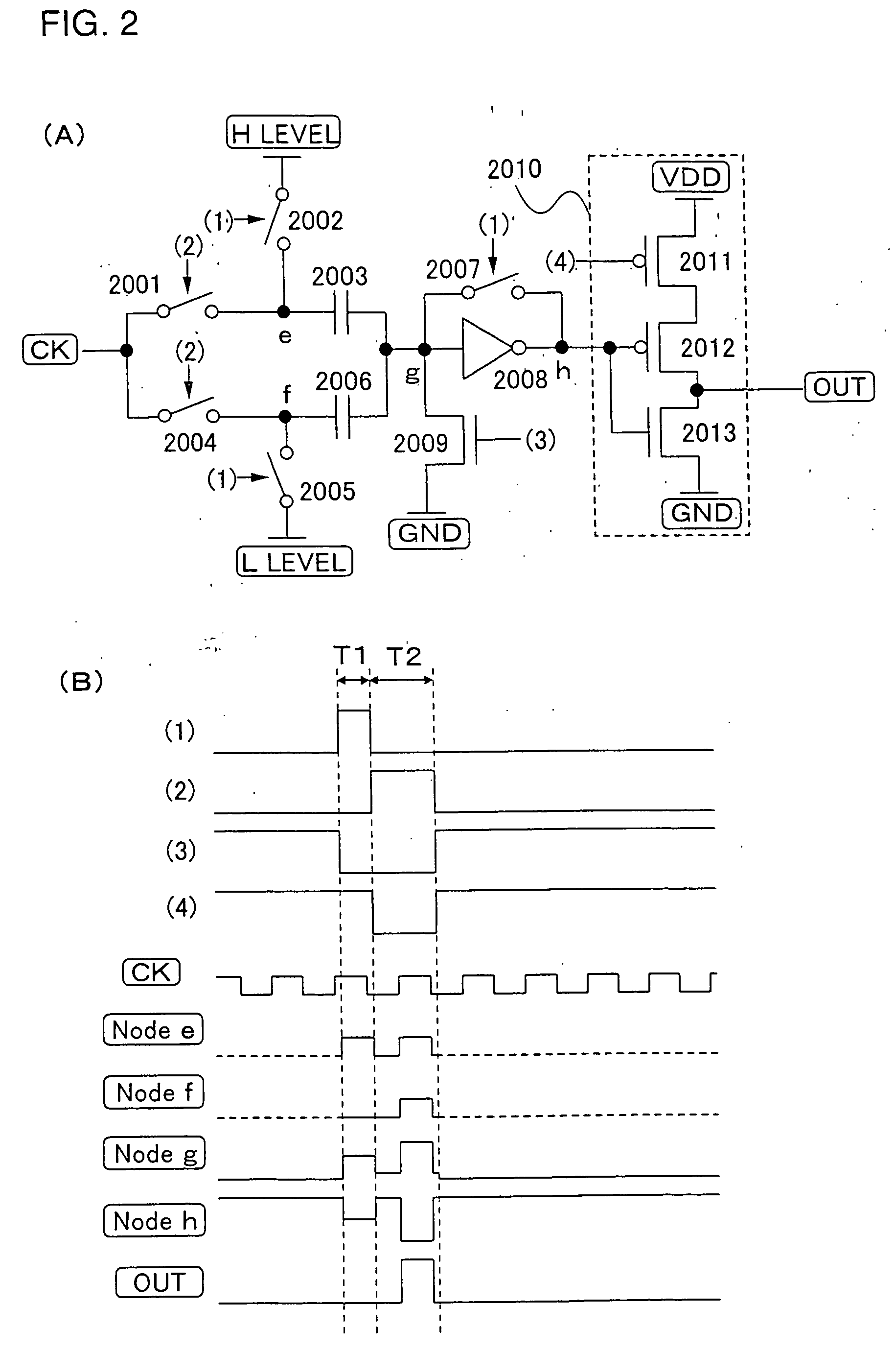
[0098]FIG. 2A shows a second structure of a level shifter which amplifies a CK signal of the shift register of the invention.

[0099] Described in Embodiment Mode 1 is the case of using the intermediate potential of a CK signal as the reference potential. In Embodiment Mode 2, a CK signal is amplified by using H-level and L-level of the CK signal as the reference potential instead of the intermediate potential.

[0100] The level shifter in this embodiment mode includes a first switch 2001 for receiving a CK signal and a second switch 2004 for receiving a CK signal, a first reference switch 2002 and a second reference switch 2005, a capacitor means 2003 for setting H-level and a capacitor means 2006 for setting L-level, a switch 2007 for setting a threshold value, a correction inverter 2008, a switch 2009 for fixing a potential, and an output inverter 2010. The output inverter 2010 includes a first P-type TFT 2011, a second P-type TFT 2012, and an N-type TFT 2013.

[0101] A capacitor me...

embodiment mode 3

[0108]FIG. 3 shows a third structure of a level shifter which amplifies a CK signal of a shift register of the invention.

[0109] In Embodiment Modes 1 and 2, a potential of an input portion of a correction inverter changes from a threshold potential by approximately half of a CK signal amplitude when a CK signal is received. Described in Embodiment Mode 3 is the case of changing the potential by the equivalent to a CK signal amplitude.

[0110] The level shifter of this embodiment mode has a first switch 3001 for receiving a CK signal and a second switch 3008 for receiving a CK signal, a first reference switch 3002 and a second reference switch 3009, a first capacitor means 3003, a second capacitor means 3007, a third capacitor means 3010, a fourth capacitor means 3014 and a fifth capacitor means 3015, a first correction inverter 3005 and a second correction inverter 3012, a first switch 3004 for setting a threshold value and a second switch 3011 for setting a threshold value, a first...


PUM


Abstract

A low power consumption shift register which inputs a CK signal with a low voltage with almost no effect of variation in characteristics of transistors. In the invention, an input portion of an inverter is set at a threshold voltage thereof and a CK signal is inputted to the input portion of the inverter through a capacitor means. In this manner, the CK signal is amplified, which is sent to the shift register. That is, by obtaining the threshold potential of the inverter, the shift register which operates with almost no effect of variation in characteristics of transistors can be provided. A level shifter of the CK signal is generated from an output pulse of the shift register, therefore, the low power consumption shift register having the level shifter which flows a shoot-through current for a short period can be provided

Description

TECHNICAL FIELD [0001] The present invention relates to an active matrix display device which displays an image by an input of a video signal. More particularly, the invention relates to a shift register which generates a sampling pulse which sequentially samples the video signal. BACKGROUND ART [0002] In recent years, an active matrix display device such as a liquid crystal display device and a light emitting device has been developed in response to the expanding demand for portable use and the like. In particular, technology for integrally forming a pixel and a driver circuit (referred to as an internal circuit, hereinafter) on an insulator by using a transistor formed by using a polycrystalline semiconductor (polysilicon) has been actively developed. An internal circuit includes a source signal line driver circuit and a gate signal line driver circuit, and controls pixels arranged in matrix. [0003] Further, the internal circuit is connected to a controller IC and the like (referr...

Claims


Application Information

Patent Timeline
Patent Type & Authority Applications(United States)
IPC IPC(8): G11C19/00G11C19/18H03K5/003H03K5/02H03K5/08H03K5/24
CPCG11C19/00G11C19/184H03K5/249H03K5/02H03K5/082H03K5/003G09G3/20H03K5/22
Inventor OSAME, MITSUAKIANZAI, AYA
Owner SEMICON ENERGY LAB CO LTD
Why Eureka
Try Eureka