Manufacturing method of semiconductor device

a manufacturing method and semiconductor technology, applied in the direction of semiconductor devices, electrical devices, transistors, etc., can solve the problems of reducing the hampered reaction between the transition metal and silicon, and the increase of the resistance of the gate electrode and the source and drain regions, so as to reduce the effect of reducing the thickness of the silicon substrate and reducing the selection ratio

Inactive Publication Date: 2005-06-23
SANYO ELECTRIC CO LTD
View PDF11 Cites 6 Cited by
  • Summary
  • Abstract
  • Description
  • Claims
  • Application Information

AI Technical Summary

Benefits of technology

[0021] This invention offers an improved method of manufacturing a semiconductor device in view of the problems described above. Dry etching and wet etching are used in etching an insulation film to form a spacer. A silicon nitride film is used as a buffer film when injecting a high dose of impurities and is removed by wet etching after the injection. Substantially larger selection ratio is made available in wet etch...

Problems solved by technology

As a manufacturing process of a semiconductor device moves to a finer design rules, there arises a problem that characteristics of a MOS transistor decline due to a short channel effect.
Another problem is resistance increase of a gate electrode and source and drain regions due to reduced dimensions of the gate electrode and the source and drain regions.
There arise following problems when a semiconductor device is manufactured by the above-mentioned technologies to form the LDD structure and the silicide layer.
Third, the reaction between the transition metal and silicon is hampered in regions where the carbon contamination has taken place, thus the silicide layer may not be formed in elliptical regions c in FIG. 14, leaving non-reacted portions ...

Method used


Image

  • Manufacturing method of semiconductor device
  • Manufacturing method of semiconductor device
  • Manufacturing method of semiconductor device

Examples


Embodiment Construction

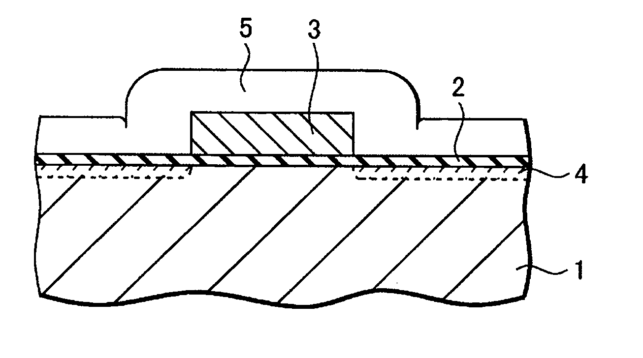
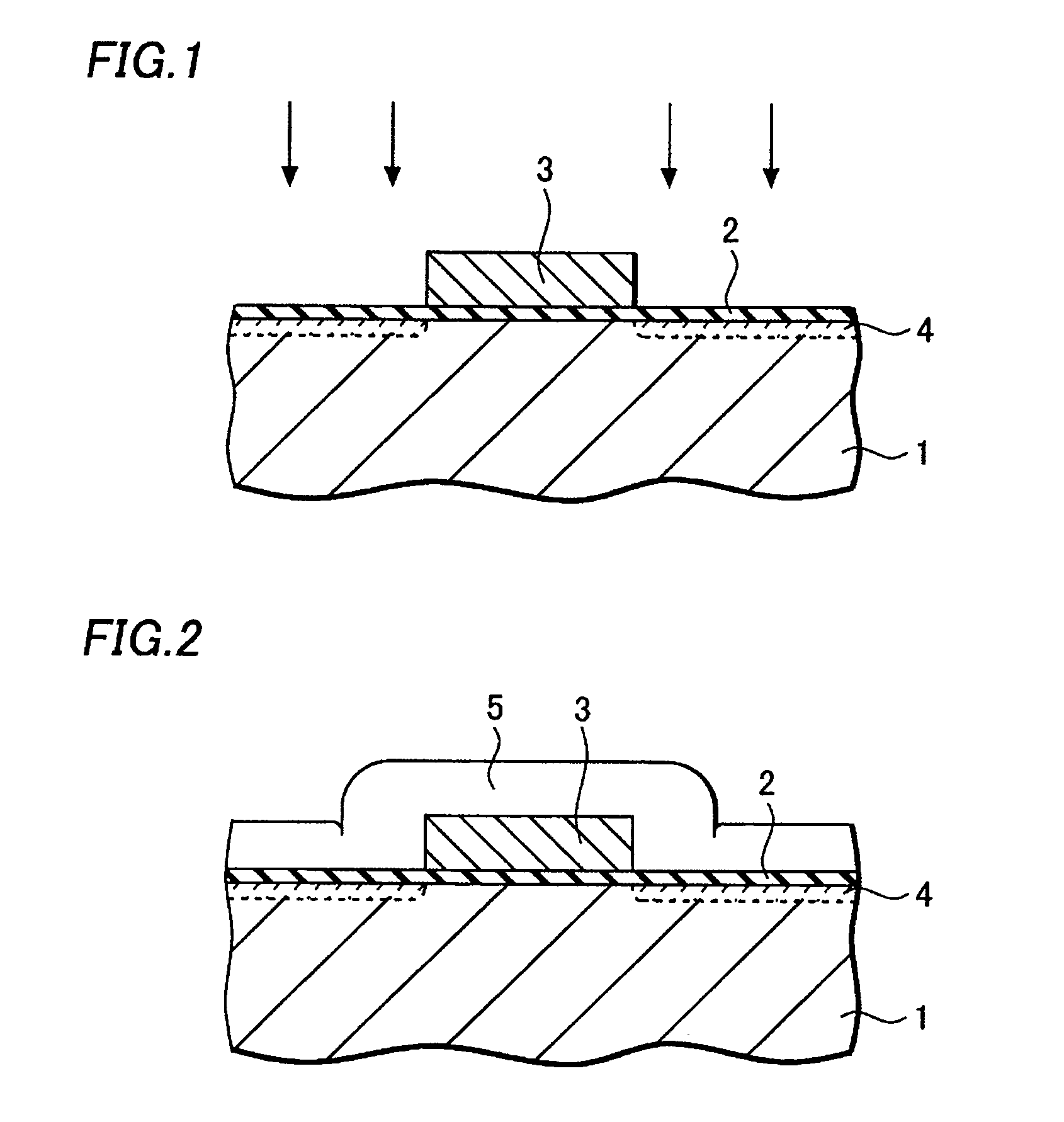
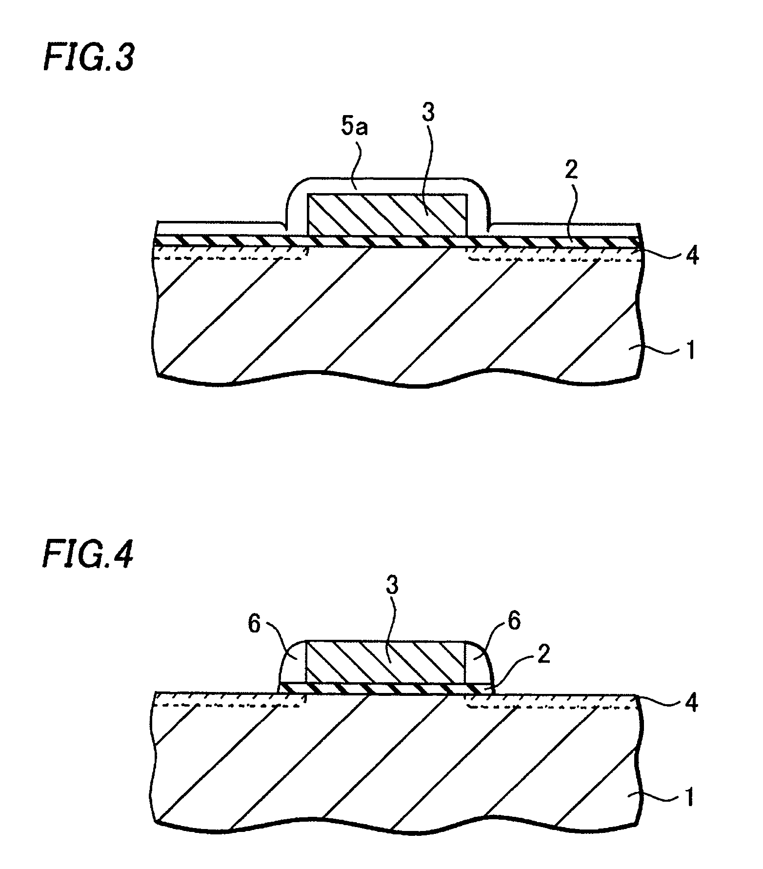
[0038] A method of manufacturing a semiconductor device according to an embodiment of this invention will be described hereafter, referring to FIGS. 1-8.

[0039] A silicon oxide film of about 5 nm in thickness is formed on a silicon substrate 1 by thermal oxidation, as shown in FIG. 1. It becomes a gate insulation film 2. A polysilicon film of about 200 nm in thickness is formed on the gate insulation film 2. A gate electrode 3 is formed by shaping the polysilicon film by photolithography and etching.

[0040] Although not shown in the figure, it should be noted that a silicon oxide film or the like may be formed on the polysilicon film and used as a hard mask to enable higher precision etching.

[0041] After that, low impurity concentration regions 4 are formed by injecting a dose of 1-5×10¹⁴ (ions / cm2) of impurity ions, e.g. phosphorus ions, into regions 10-20 mn deep from a surface of the silicon substrate 1, using the gate electrode 3 as a mask. After the injection, N2 annealing, i....


PUM


Abstract

An LDD structure and a silicide layer are formed without a reduction in thickness of a silicon substrate or a carbon contamination. Forming a spacer on a sidewall of a gate electrode is performed in two process steps, i.e. dry-etching and wet-etching. Also, a silicon nitride film used as a buffer film in injection of high dose of impurities is removed by wet-etching. As a result, the reduction in thickness of the silicon substrate and the carbon contamination can be prevented. In addition, variation in depth of the high and low impurity concentration regions and silicide forming region with locations on the wafer can be suppressed because of high selection ratio available with the wet-etching.

Description

CROSS-REFERENCE OF THE INVENTION [0001] This invention is based on Japanese Patent Application No. 2003-369269, the content of which is incorporated herein by reference in its entirety. BACKGROUND OF THE INVENTION [0002] 1. Field of the Invention [0003] This invention relates to a manufacturing method of a semiconductor device, specifically to a manufacturing method of a semiconductor device having an LDD (Lightly Doped Drain) structure and silicide layers formed on a silicon substrate and a gate electrode. [0004] 2. Description of the Related Art [0005] As a manufacturing process of a semiconductor device moves to a finer design rules, there arises a problem that characteristics of a MOS transistor decline due to a short channel effect. A technology called LDD has been developed and used as a countermeasure against the problem. Another problem is resistance increase of a gate electrode and source and drain regions due to reduced dimensions of the gate electrode and the source and d...

Claims


Application Information

Patent Timeline
IPC IPC(8): H01L21/02H01L21/265H01L21/28H01L21/336H01L21/8234H01L21/84H01L29/78
CPCH01L21/2652H01L29/7833H01L29/6659H01L29/665
Inventor IIZUKA, KATSUHIKOOKADA, KAZUOMORI, TOMONORIDOBASHI, HIROYUKISUZUKI, HIROYUKIHONDA, TAKAYOSHITANIGUCHI, TOSHIMITSU
Owner SANYO ELECTRIC CO LTD
Why Eureka
Try Eureka