Infrared ray detecting type imaging device

a technology of infrared ray detection and imaging device, which is applied in the direction of radiation controlled devices, optical radiation measurement, instruments, etc., can solve the problems of metal wiring such as aluminum wiring deterioration, limited material usable for bolometer films, and deterioration of transistor characteristics

Inactive Publication Date: 2005-06-30
KK TOSHIBA
View PDF23 Cites 10 Cited by
  • Summary
  • Abstract
  • Description
  • Claims
  • Application Information

AI Technical Summary

Benefits of technology

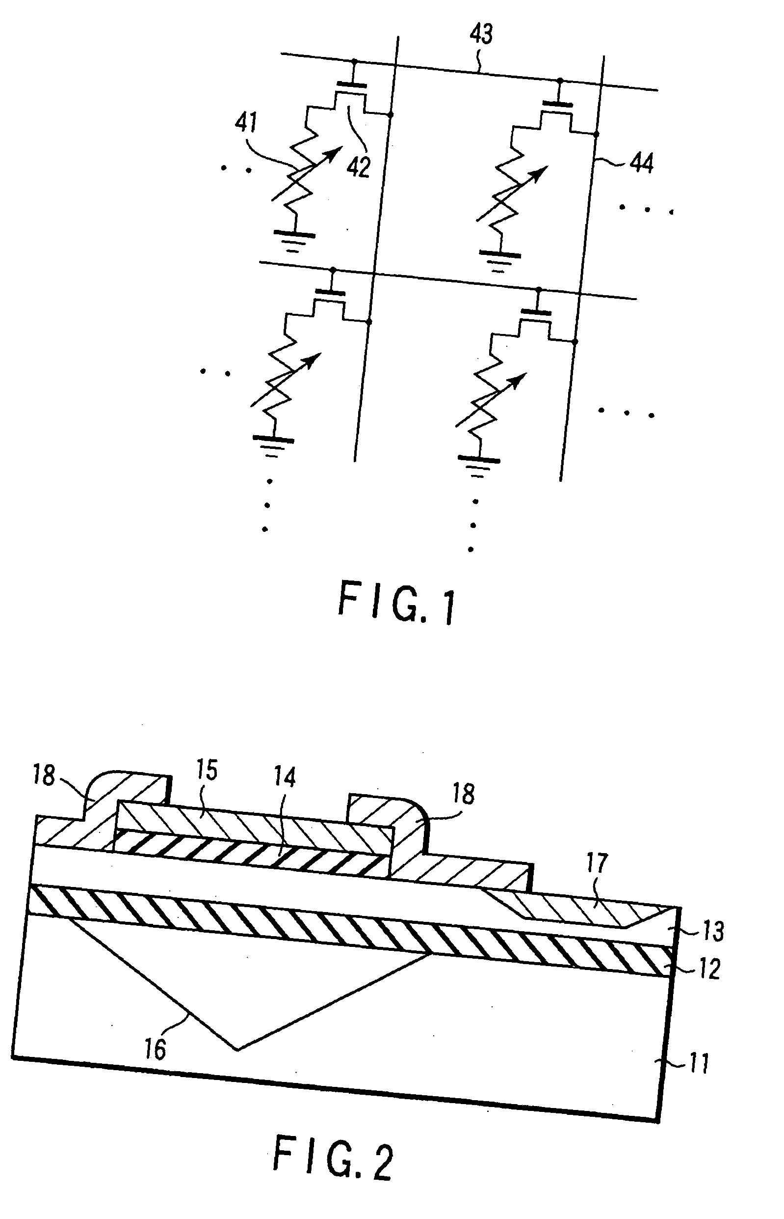
[0010] A second aspect of the invention, there is provided an imaging device comprising: a first select line; a first signal line crossing the first select line; a first pixel provided at a portion corresponding to a crossing portion of the first select line and the first signal line, the first pixel comprising a first bolometer film generating a first temperature detection signal, and a first switching element selected by a first select signal from the first select line and supplying the first temperature detection signal to the first signal line; a second signal line crossing the first select line; a second pixel provided at a portion corresponding to a crossing portion of the first select line and the second signal line, the second pixel comprising a second bolometer film generating a second temperature detection signal, and a second switching element selected by the first select signal and supplying the second temperature detection signal to the second signal line; and a control circuit controlling a width of the first select signal in accordance with the second temperature detection signal.

Problems solved by technology

If the process temperature is higher, the metal wiring such as an aluminum wiring deteriorates.
Further, by heat treatment at high temperature of about 800° C. or more, the transistor characteristic also deteriorates.
Therefore, in the conventional infrared imaging device, materials usable for the bolometer film are limited.
At these positions of steps and contact holes, the bolometer film has crystal disturbance and grain boundary, which causes noise or characteristic deterioration.
Therefore, in the conventional infrared imaging device, since the bolometer film must be formed at a relatively low temperature, materials for the bolometer film are limited.
Besides, by the undulations existing beneath the bolometer film, noise and characteristic deterioration are caused.
It was hence difficult to obtain an infrared imaging device of high performance.

Method used


Image

  • Infrared ray detecting type imaging device
  • Infrared ray detecting type imaging device
  • Infrared ray detecting type imaging device

Examples


example 1

[0089] A thin film of Sm1-xAxNiyO3-d was fabricated by a molecular beam epitaxy (MBE) method.

[0090]FIG. 10 schematically shows a configuration of a molecular beam epitaxy apparatus.

[0091] As shown in FIG. 10, gas in a vacuum chamber 81 is exhausted by a cryopump. A substrate holder 82 is provided in the vacuum chamber 81, and a substrate 83 is placed on the substrate holder 82. The substrate holder 82 is heated by a heater 84.

[0092] Opposite to the substrate 83, plural Knudsen cells 85 are disposed, and a cell shutter 86 is provided with each Knudsen cell 85. Each Knudsen cell 85 is filled with constituent element of thin film formed in the following examples, that is, La, Al, Sm, Ni, Bi and Nd. Further, to obtain a thin oxide film, pure ozone gas (O3 gas) stored in a liquid ozone bath 87 is injected from a nozzle 88, and supplied to the substrate 83. To form a proper thin film of Sm1-xAxNiyO3-d, Ni3+ is needed, and a strong oxidizing condition is required. In this example, Ni3+ ...

example 2

[0101] A thin film of Ca2RuO4 was formed by RF sputtering method.

[0102] Using a Ca2RuO4 sinter target of 4 inches in diameter, RF power of 60 W was applied. The sputtering gas was a mixed gas of Ar 90%+O2 10%, the flow rate was 33 sccm, and the pressure was 1 Pa. The substrate temperature was room temperature.

[0103] Substrates were SrTiO3 (100) single crystal substrate, NdGaO3 (001) single crystal substrate, and LaAlO3 (100) single crystal substrate. As a result, only in the case of using LaAlO3 substrate and annealing at temperature of 975° C. or more after forming the film, Ca2RuO4 having a desired K2NiF4 type crystal structure was obtained.

[0104]FIG. 15 shows the heat treatment temperature dependence of Ca2RuO4 (002) peak intensity of X-ray diffraction. When heated at 990° C. or more and 1050° C. or less, Ca2RuO4 of excellent crystallinity was obtained. If heated at 1050° C. or more, Ca3Ru2O7 was mixed as impurity phase. When heated at less than 990° C., the amount of CaRuO3 i...


PUM


Abstract

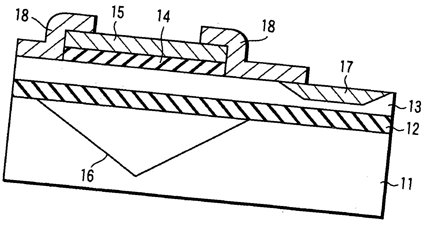
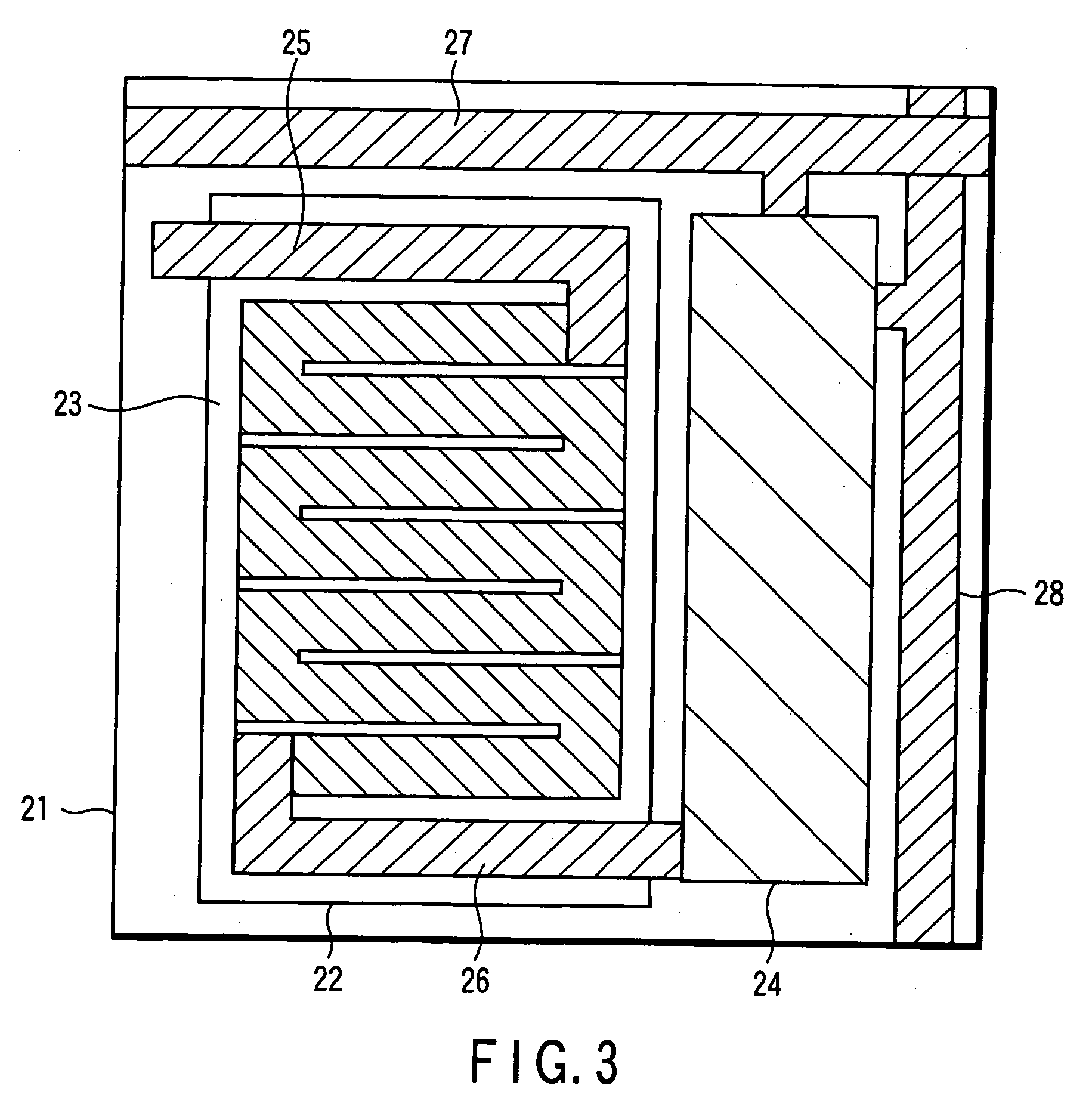
An imaging device comprises a select line, a first signal line crossing the select line, and a first pixel provided at a portion corresponding to a crossing portion of the select line and the first signal line, the first pixel comprising a first buffer layer formed on a substrate, a first bolometer film formed on the first buffer layer, made of a compound which undergoes metal-insulator transition, and generating a first temperature detection signal, a first switching element formed on the substrate, selected by a select signal from the select line, and supplying the first temperature detection signal to the first signal line, and a metal wiring connecting a top surface of the first bolometer film to the first switching element.

Description

CROSS-REFERENCE TO RELATED APPLICATIONS [0001] This application is based upon and claims the benefit of priority from the prior Japanese Patent Application No. 2002-81795, filed Mar. 22, 2002, the entire contents of which are incorporated herein by reference. BACKGROUND OF THE INVENTION [0002] 1. Field of the Invention [0003] The present invention relates to an imaging device and a method of manufacturing the same, and more particularly to an infrared ray detecting type imaging device (an infrared imaging device) and a method of manufacturing the same. [0004] 2. Description of the Related Art [0005] An infrared imaging device is proposed, in which a bolometer film is formed on a semiconductor substrate on which a circuit including transistor and wiring and the like is formed. This device detects an infrared ray for each pixel by making use of change of a resistance value of the bolometer film depending on temperature, and reads the detected signal by way of the transistor. In the co...

Claims


Application Information

Patent Timeline
Patent Type & Authority Applications(United States)
IPC IPC(8): G01J1/02G01J1/42G01J1/44G01J5/00G01J5/20G01J5/22G01J5/24G01J5/48H01L27/14H01L27/144H01L27/16H01L37/00H04N5/33H04N5/335H04N5/369
CPCG01J5/20G01J5/22H04N5/33G01J2005/202H01L27/16G01J5/24H10N19/00
Inventor IKEGAWA, SUMIONAKAYAMA, KOHEIFUNAKI, HIDEYUKIIIDA, YOSHINORISHIGENAKA, KEITARO
Owner KK TOSHIBA
Why Eureka
Try Eureka