Electronic device and method of manufacturing the same

a technology of electronic devices and manufacturing methods, applied in the field of electronic devices, can solve the problems of limiting the application of conventional framing and damage to elements that have already been formed, and achieve the effects of reducing oxidation problems, high quality framing, and enhancing the transparency of electronic devices

Active Publication Date: 2005-06-30
SAMSUNG ELECTRONICS CO LTD
View PDF7 Cites 10 Cited by
  • Summary
  • Abstract
  • Description
  • Claims
  • Application Information

AI Technical Summary

Benefits of technology

[0047] Further, since a diffusion barrier layer is unnecessary, it is possible to eliminate the oxidation problem. As a result, high quality FRAM can be obtained. Further, since the thin film transistors and the ferroelectric capacitors may be formed on a transparent substrate, the transparency of an electronic device can be realized, thereby increasing its usefulness for a variety of applications.

Problems solved by technology

Also, since the conventional FRAM is formed using CMOS processes, it is difficult to form a transparent FRAM, thus limiting the applications of the conventional FRAM.
Further, since the conventional FRAM is formed using high temperature processes, elements that have already been formed may be damaged during the high temperature processes.

Method used


Image

  • Electronic device and method of manufacturing the same
  • Electronic device and method of manufacturing the same
  • Electronic device and method of manufacturing the same

Examples


first device embodiment

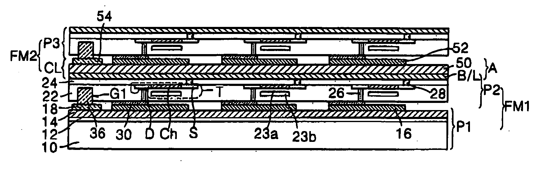
[0081] Referring to FIG. 1, an FRAM according to a first device embodiment of the present invention includes a capacitor part P1 and a switching element part P2, which are bonded with each other. The capacitor part P1 includes a capacitor C provided below the switching element part P2. The capacitor C serves as the functional element for the FRAM. The capacitor part P1 includes a first substrate 10. First electrodes 12, a dielectric layer 14, and second electrodes 16 are sequentially stacked on the first substrate 10, thereby forming the capacitor C. There are a plurality of first electrodes 12 and second electrodes 16 defining each capacitor C. The first and second electrodes 12 and 16 are perpendicular to one another. The first electrode 12 and the second electrode 16 are an upper electrode and a lower electrode of the capacitor C, respectively.

[0082] The first substrate 10 may be a transparent substrate, e.g., a sapphire substrate or a glass substrate. The first and second elect...

second device embodiment

[0088] A second device embodiment includes two or more FRAM stacked layers. At least one of the stacked FRAM layers may be the same as the FRAM shown in FIG. 1.

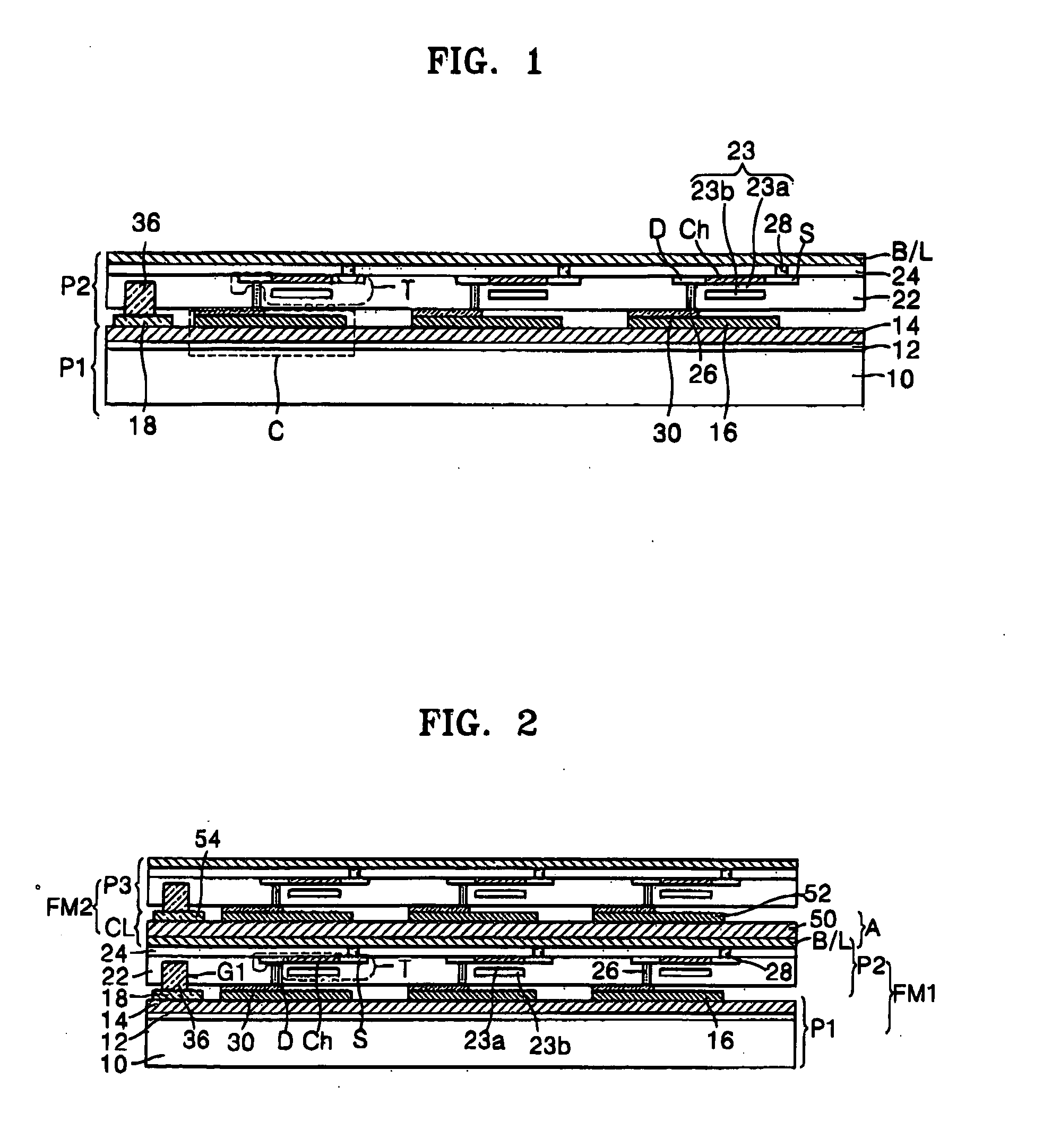
[0089] Referring to FIG. 2, an FRAM according to the second device embodiment of the present invention may include first and second FRAM layers FM1 and FM2, which are stacked in sequence. A structure of the first FRAM layer FM1 is identical to that of the FRAM of FIG. 1, which includes the capacitor part P1 and the switching element part P2. The second FRAM layer FM2 includes a capacitor layer CL and a switching element part P3 which are sequentially stacked.

[0090] The capacitor layer CL includes a lower electrode 48 (shown in FIG. 3), a ferroelectric layer 50, and an upper electrode 52, which are sequentially stacked. A third bonding pad 54 is provided on the ferroelectric layer 50, preferably at an edge portion. The switching element part P3 may be identical to the switching element part P2 of the first FRAM layer FM1. Ho...

third device embodiment

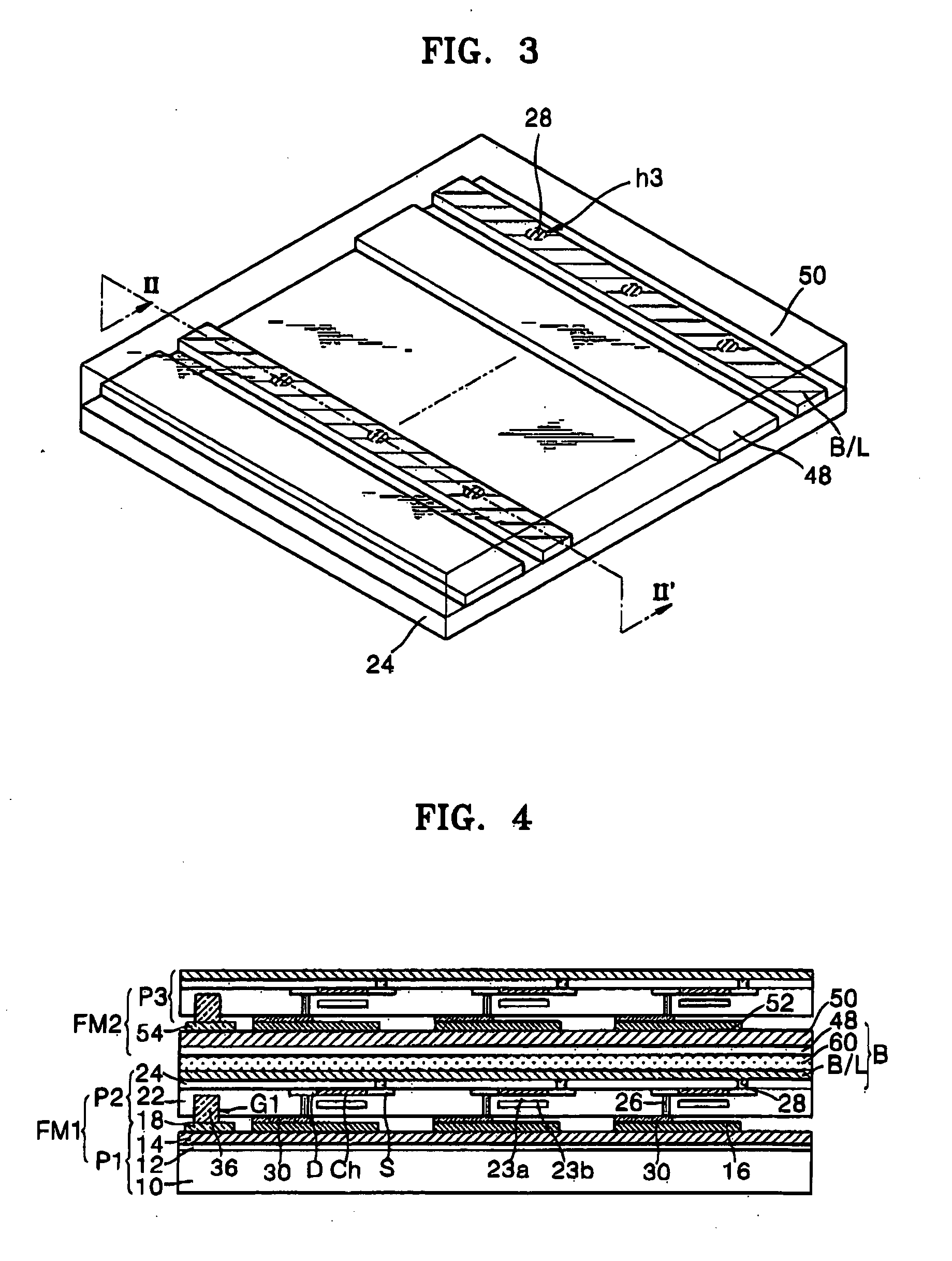
[0096] As shown in FIG. 4, a third device embodiment relates to an FRAM that includes an interlayer insulating layer 60 between a first FRAM layer FM1 and a second FRAM layer FM2. Referring to FIG. 4, since the interlayer insulating layer 60 is formed between the first and second FRAM layers FM1 and FM2, the lower electrode 48 of the second FRAM layer FM2 and the bit line B / L of the first FRAM layer FM1 are provided in different planes.

[0097]FIG. 5 illustrates a side view of a stacked structure B of FIG. 4, which includes a portion of the first FRAM layer FM1 and a portion of the second FRAM layer FM2 on respective sides of the interlayer insulating layer 60.

[0098] Referring to FIG. 5, a plurality of bit lines B / L are provided on the second substrate 24 and the interlayer insulating layer 60 covers the bit lines B / L. Lower electrodes 48 are formed on the interlayer insulating layer 60. The lower electrodes 48 are arranged in parallel with the bit lines B / L.

[0099] In this manner, ...


PUM


Abstract

In an electronic device, and a method of manufacturing the same, the electronic device includes a first substrate, a first lower capacitor on the first substrate, a first lower switching element on the first lower capacitor, and a second substrate on the first lower switching element. The electronic device may further include a second lower switching element which is isolated from the first lower capacitor, and an upper capacitor on the second substrate, the lower electrode of the upper capacitor being connected to the second lower switching element.

Description

BACKGROUND OF THE INVENTION [0001] 1. Field of the Invention [0002] The present invention relates to an electronic device and a method of manufacturing the same. More particularly, the present invention relates to an electronic device in which a functional element and a switching element are bonded vertically, and a method of manufacturing the same. [0003] 2. Description of the Related Art [0004] Among electronic devices, memory devices are used in almost all electronic equipment. Demand for nonvolatile memory devices continues to increase. [0005] Nonvolatile memory devices include a ferroelectric random access memory (FRAM). An FRAM includes one metal oxide semiconductor (MOS) transistor and one ferroelectric capacitor. The ferroelectric capacitor includes a lower electrode, a ferroelectric layer and an upper electrode, which are stacked in sequence. The ferroelectric layer is stacked on the lower electrode in an amorphous state. Thus, after the ferroelectric layer is formed, an an...

Claims


Application Information

Patent Timeline
Patent Type & Authority Applications(United States)
IPC IPC(8): G11C11/22H01L21/3205H01L21/82H01L21/8239H01L21/8246H01L21/84H01L27/10H01L27/105H01L27/115H01L27/12H01L29/786H01L31/119
CPCH01L21/84H01L27/12H01L27/11507H01L27/11502H10B53/30H10B53/00H01L27/105
Inventor XIANYU, WENXUNOGUCHI, TAKASHIYOO, IN-KYEONGPARK, YOUNG-SOO
Owner SAMSUNG ELECTRONICS CO LTD
Why Eureka
Try Eureka