Method for manufacturing an organic semiconductor element

a technology of organic semiconductor elements and manufacturing methods, which is applied in the direction of instruments, optics, solid-state devices, etc., can solve the problems of reducing the characteristic of tft, achieve the effects of reducing leakage current at off-state, improving the characteristic of organic semiconductor elements, and enhancing the flexibility and lightweight of liquid crystal display devices or display devices having light emitting elements

Inactive Publication Date: 2005-06-30
SEMICON ENERGY LAB CO LTD
View PDF24 Cites 45 Cited by
  • Summary
  • Abstract
  • Description
  • Claims
  • Application Information

AI Technical Summary

Benefits of technology

[0012] Moreover, an organic semiconductor has a disadvantage in which an organic semiconductor is deteriorated due to moisture or atmospheric air in the case of being left in atmospheric air; and thus TFT characteristic is decreased. Furthermore, characteristic of an organic semiconductor element is influenced by the adhesion strength between an organic semiconductor film and an electrode, and between the organic semiconductor film and an insulating film.
[0013] In view of the foregoing problems, it is an object of the invention to provide a method for manufacturing an organic semiconductor element which can prevent TFT characteristic from deteriorating even if an element in which a channel length is short or a channel width is narrow.
[0026] Furthermore, the organic semiconductor element formed in the above-mentioned manner can be obtained and the organic semiconductor element can be provided for a pixel portion of a liquid crystal display device or a display device having a light emitting element to use as a semiconductor element according to the invention. Especially, flexibility and lightweight of the liquid crystal display device or the display device having a light emitting element can be enhanced by providing the organic semiconductor element over synthetic resin.
[0027] According to the invention, a threshold value of ON-OFF can be changed and leakage current at OFF state can be reduced. Thus, the threshold value of ON-OFF can be made close to 0V to raise ON-OFF ratio. Accordingly, characteristic of the organic semiconductor element can be improved.
[0028] Moreover, due to the improvement, practicable TFT characteristic can be obtained even if an element in which a channel length is short and a channel width is narrow is used, and thus a device such as a display device can be downsized.

Problems solved by technology

Moreover, an organic semiconductor has a disadvantage in which an organic semiconductor is deteriorated due to moisture or atmospheric air in the case of being left in atmospheric air; and thus TFT characteristic is decreased.

Method used


Image

  • Method for manufacturing an organic semiconductor element
  • Method for manufacturing an organic semiconductor element
  • Method for manufacturing an organic semiconductor element

Examples


embodiment

[0044] Embodiment Mode 1

[0045] In this embodiment mode, a method for manufacturing an organic TFT is described as an organic semiconductor element of bottom contact type.

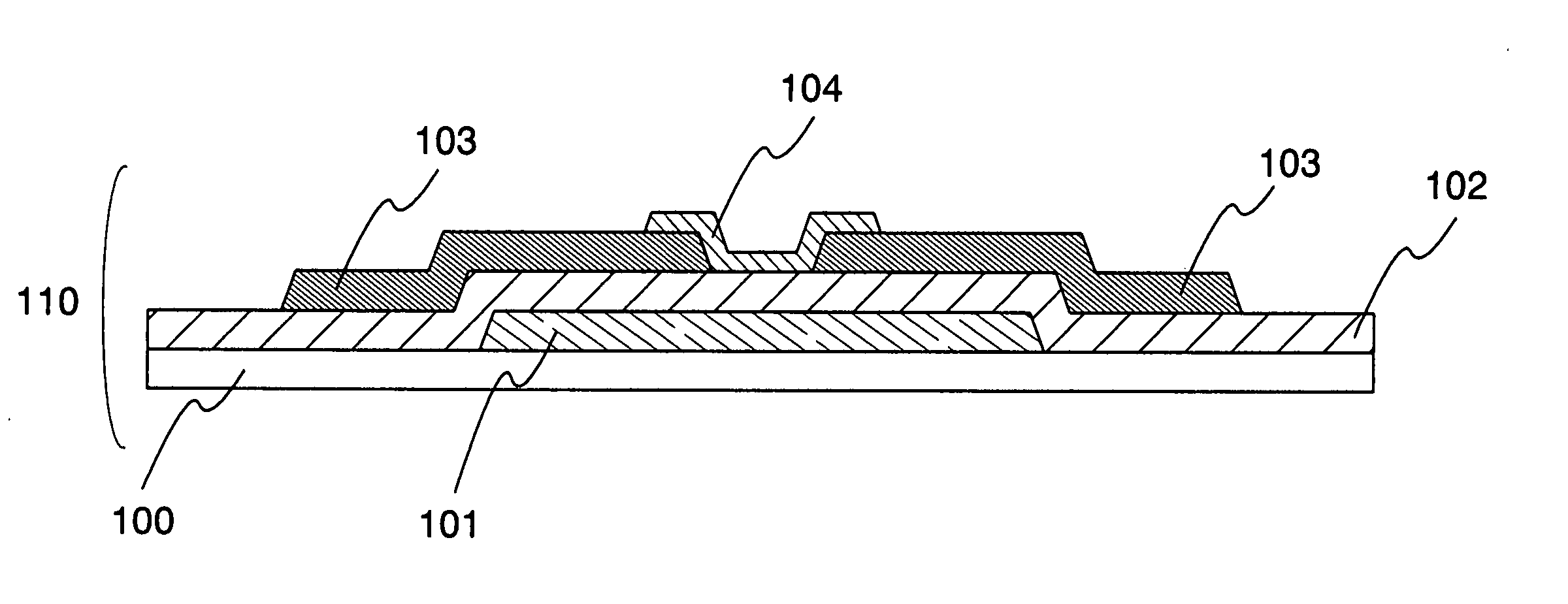
[0046]FIG. 1 shows a cross-sectional view of an organic TFT of bottom contact type. The organic TFT of bottom contact type has an element structure in which an organic semiconductor film is formed after a source electrode and a drain electrode are formed.

[0047] First, a conductive film (hereinafter, a gate electrode) 101 which serves as a gate electrode is formed over a substrate 100 having an insulating surface. Note that a method for manufacturing an organic TFT in this embodiment mode is illustrated with an example in which a quartz substrate is used for the substrate 100 having an insulating surface, tungsten (W) is used as the conductive film 101 over the quartz substrate, and the gate electrode is formed by a sputtering method, but the present invention is not limited to this.

[0048] As a substrate having an...

embodiment 1

[0087] Embodiment 1

[0088] In this embodiment, a result which is temperature dependence of electric properties of the organic TFT manufactured by performing baking under atmospheric pressure according to the above-mentioned Embodiment Mode 1 is shown. Note that the organic TFT used as a test sample has a structure in which a gate electrode 301 formed by tungsten is provided over a quartz substrate, a gate insulating film is provided over the gate electrode 301, a source electrode 302 and a drain electrode 303 formed by tungsten are provided over the gate insulating film, and an organic semiconductor film is provided between the source electrode 302 and the drain electrode 303, in atmospheric air as shown FIG. 3. Moreover, the source electrode 302, the drain electrode 303 and the gate electrode 301 is each provided with a measuring pad (a pad 304 for the source electrode, a pad 305 for the drain electrode, a pad 306 for the gate electrode) to apply measurement voltage or to detect cur...

embodiment 2

[0101] Embodiment 2

[0102] In this embodiment, a result which is time dependence of electric properties of the organic TFT manufactured by performing baking under atmospheric pressure according to the above-mentioned Embodiment Mode 1 is shown. Note that a manufacturing condition of the organic TFT, other than the baking condition after deposition, used as a test sample is the same as in Embodiment 1.

[0103] The baking condition after deposition is as follows: [0104] (1) Before baking after deposition [0105] (2) Baking (1) at a temperature of 120° C. for 10 minutes under atmospheric pressure [0106] (3) Baking (2) at a temperature of 120° C. for 30 minutes under atmospheric pressure

[0107]FIG. 5 shows a result of Vg-Id characteristic in which the current of the drain electrode and gate voltage are detected when voltage of −10V is applied as Vd in the baking condition (1) through (3).

[0108]FIG. 5 shows that a threshold value of ON-OFF approaches 0V by performing baking after depositio...


PUM

PropertyMeasurementUnit
temperatureaaaaaaaaaa
temperaturesaaaaaaaaaa

Abstract

In manufacturing a device using an organic TFT, it is essential to develop an element in which a channel length is short or a channel width is narrow to downsize a device. Based on the above, it is an object of the present invention to provide an organic TFT in which characteristic is improved. In view of the foregoing problem, one feature of the present invention is that an element is baked after an organic semiconductor film is deposited. More specifically, one feature of the present invention is that the organic semiconductor film is heated under atmospheric pressure or under reduced pressure. Moreover, a baking process may be carried out in an inert gas atmosphere.

Description

BACKGROUND OF THE INVENTION [0001] 1. Field of the Invention [0002] The present invention relates to an organic semiconductor element having an organic semiconductor film and a method for manufacturing thereof. [0003] 2. Description of the Related Art [0004] In recent years, a display device provided with a thin film transistor (hereinafter, a TFT) having a thin film semiconductor has been studied and put into practical use. A high-resolution display device can be achieved since a large number of pixels can be constituted in the display device provided with a TFT. Moreover, the display device provided with a TFT can be operated in low power consumption compared with a CRT. Furthermore, the display device provided with a TFT occupies small space, since a display can be made without using a large-sized display tube like a CRT. Thus, the display device provided with a TFT has been widely used for a display portion of a personal computer, a PDA, a TV, or the like. [0005] A display devic...

Claims


Application Information

Patent Timeline
Patent Type & Authority Applications(United States)
IPC IPC(8): G02F1/1368H01L51/00H01L51/30H01L51/40
CPCB82Y30/00G02F1/1368G02F2202/025H01L51/0002H01L51/0034H01L51/0545H01L51/0036H01L51/0038H01L51/0051H01L51/0053H01L51/0035H10K71/10H10K85/10H10K85/114H10K85/111H10K85/611H10K85/113H10K85/621H10K10/466
Inventor HIRAKATA, YOSHIHARUISHITANI, TETSUJIFUKAI, SHUJIIMAHAYASHI, RYOTA
Owner SEMICON ENERGY LAB CO LTD
Why Eureka
Try Eureka