Method of forming a metal silicide layer on non-planar-topography polysilicon

a polysilicon and metal silicide technology, applied in the field of metal silicide layer formation, can solve the problems of poor bottom coverage and poor sidewall coverage, and achieve the effects of reducing the stress and resistance of the silicide layer, facilitating the formation of a metal silicide layer, and rapid thermal processing

Active Publication Date: 2005-07-07
MACRONIX INT CO LTD
View PDF6 Cites 19 Cited by
  • Summary
  • Abstract
  • Description
  • Claims
  • Application Information

AI Technical Summary

Benefits of technology

[0007] Briefly, various methods can facilitate the formation of a metal silicide layer on polysilicon, wherein the polysilicon has a non-planar topography including, for example, features. Initially, non-planar topography polysilicon is formed on a substrate. A metal layer is then deposited on the substrate using a plurality of metal depositions. A first rapid thermal processing (RTP) step then forms a silicide layer at an interface between the metal layer and the non-planar topography polysilicon. The formation of this silicide layer occurs during the first RTP step as a result of the transformation of a reactive part of the metal layer (i.e., a portion of the metal layer that is in physical contact with the polysilicon) into silicide. After the first RTP step, a wet etch, such as a selective wet etch, removes an un-reactive part of the metal layer. A second RTP step is then implemented to reduce a stress and resistance of the silicide layer.

Problems solved by technology

When a layer of polysilicon has a non-planar topography, using conventional physical vapor deposition (PVD) to deposit the metal layer can result in poor bottom coverage, meaning that either the metal layer is not deposited onto the low points of the topography or the metal layer that may exist at those low points is thin compared to the metal layer deposited onto the higher points of the topography.
Likewise, to the extent a metal deposition process were to be accomplished through ionized metal plasma physical vapor deposition (IMP PVD) with a biased wafer chuck, the bottom coverage may be exceptional, but the sidewall coverage may be poor.

Method used


Image

  • Method of forming a metal silicide layer on non-planar-topography polysilicon
  • Method of forming a metal silicide layer on non-planar-topography polysilicon
  • Method of forming a metal silicide layer on non-planar-topography polysilicon

Examples


second embodiment

VD, and then Biased IMP or CD

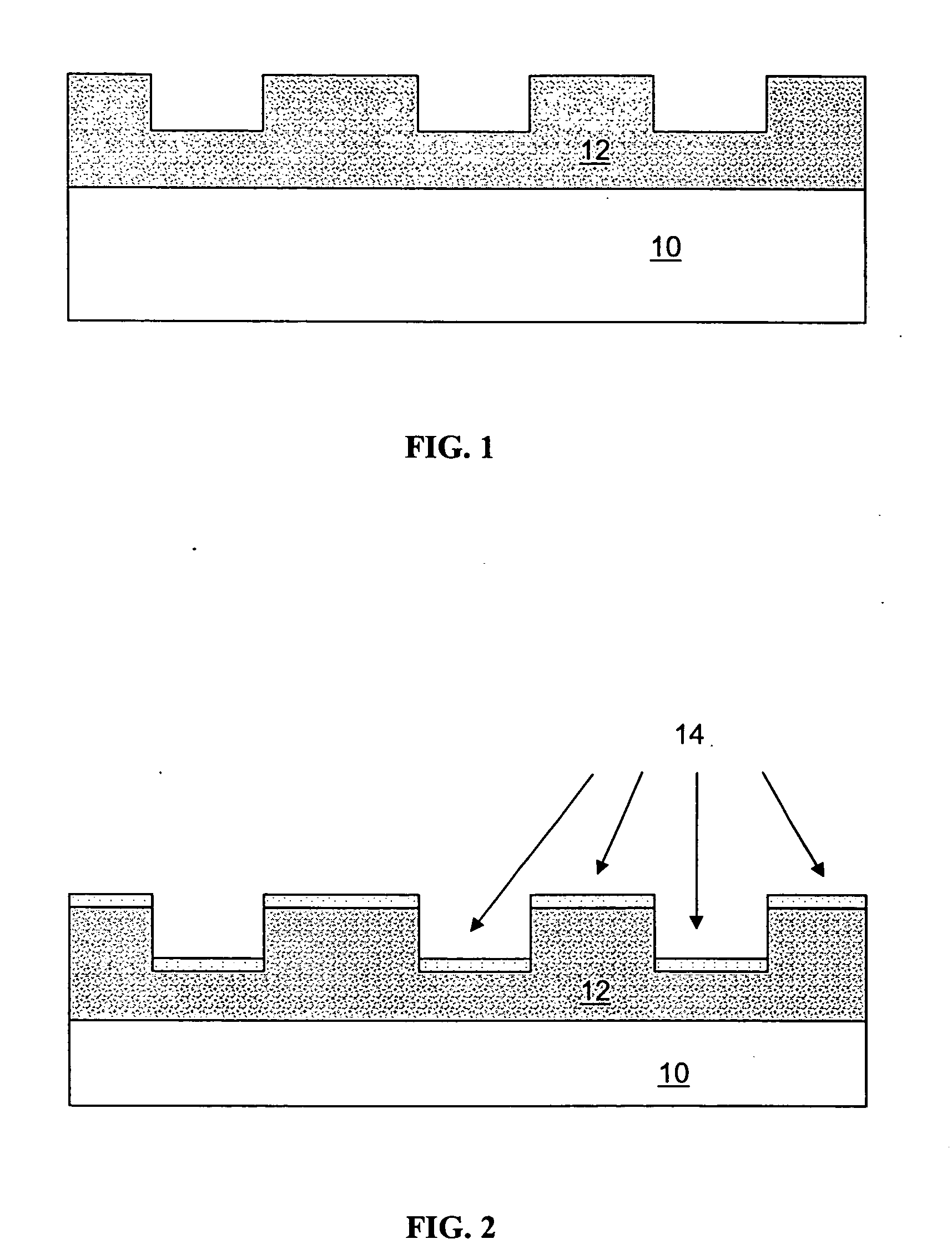
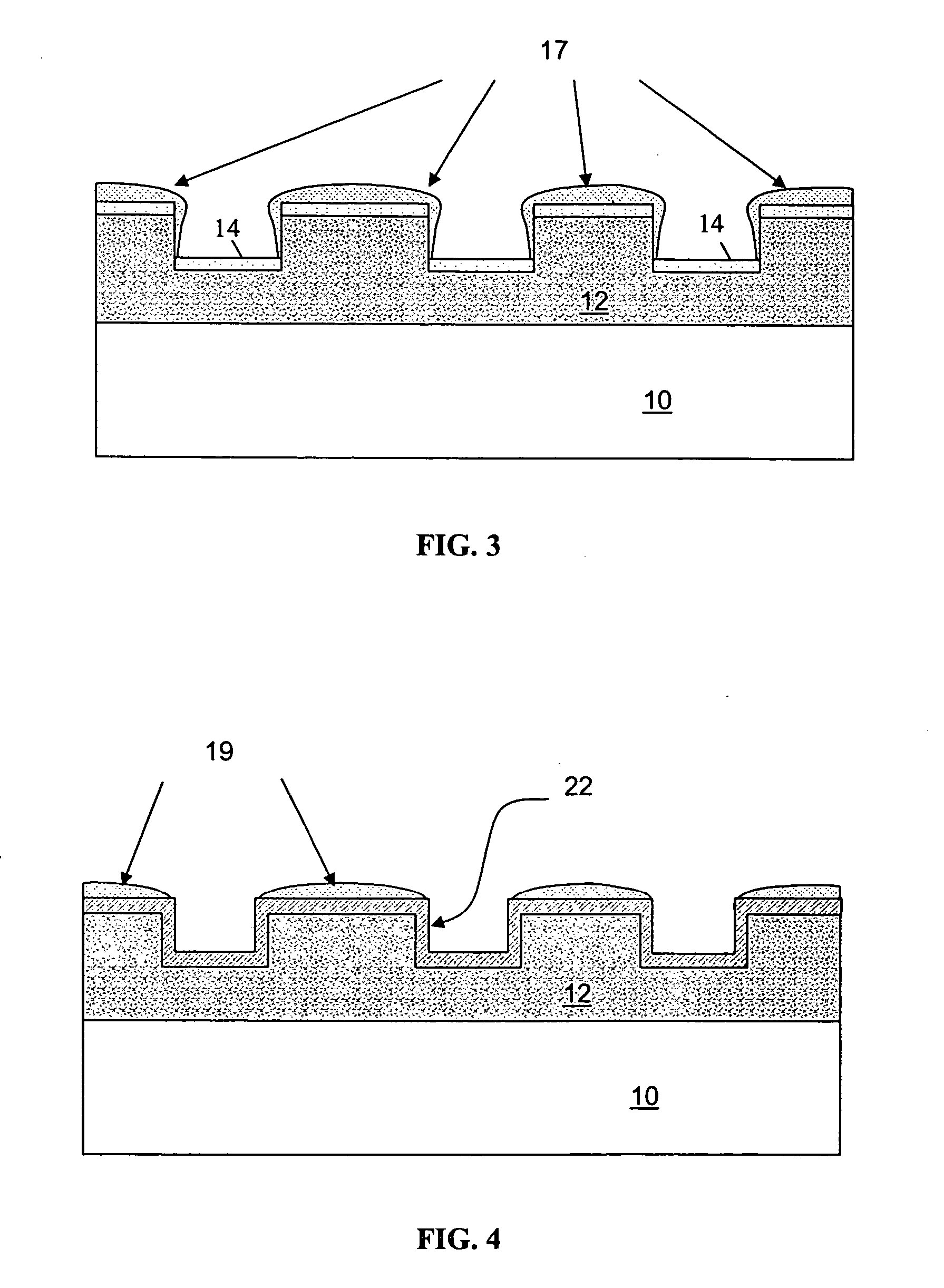
[0051] In a second embodiment, the order of the two metal depositions described in the first embodiment is changed. According to one embodiment, the order of the two metal deposition process steps is the only difference between the second illustrated embodiment and the first illustrated embodiment. Hence, in a first step in a semiconductor process, non-planar topography or featured polysilicon is formed on a substrate.

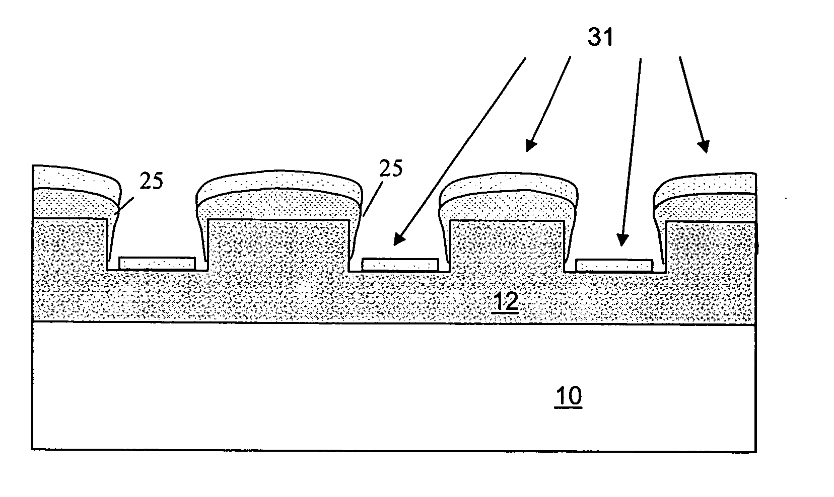
[0052] In a subsequent step in the semiconductor process, a first metal layer is formed on the substrate by an improving sidewall coverage process. FIG. 6 is a schematic diagram of a semiconductor profile depicting a step in a semiconductor process, in accordance with this second illustrated embodiment of the present invention, wherein the first metal layer 25 is deposited onto the top, the sides and slightly on the bottom of the non-planar topography polysilicon 12. The first metal layer 25 is formed, for example, by either unbiased IMP d...


PUM

PropertyMeasurementUnit
temperaturesaaaaaaaaaa
aspect ratiosaaaaaaaaaa

Abstract

A process is described for creating a uniformly thick layer of titanium, cobalt, or nickel silicide over a layer of polysilicon that has features or a non-planar topography. A dual layer of metal is deposited onto patterned polysilicon such that the first layer covers the bottoms and tops of the non-planar topography and the second layer covers the sidewalls and tops of the non-planar topography. By heating the metal, etching away any un-reacted metal, and heating the result a second time, a metal silicide layer of uniform thickness, reduced stress and reduced resistivity is formed.

Description

BACKGROUND OF THE INVENTION [0001] 1. Field of the Invention [0002] The present invention relates generally to semiconductor processing and, more particularly, to the formation of a metal silicide layers. [0003] 2. Description of Related Art [0004] A known method of forming a metal silicide layer on polysilicon comprises depositing a metal layer on the polysilicon, performing a first rapid thermal processing (RTP) step, performing a wet etch, and then performing a second RTP step. [0005] When a layer of polysilicon has a non-planar topography, using conventional physical vapor deposition (PVD) to deposit the metal layer can result in poor bottom coverage, meaning that either the metal layer is not deposited onto the low points of the topography or the metal layer that may exist at those low points is thin compared to the metal layer deposited onto the higher points of the topography. Likewise, to the extent a metal deposition process were to be accomplished through ionized metal pla...

Claims


Application Information

Patent Timeline
Patent Type & Authority Applications(United States)
IPC IPC(8): C23C14/04C23C14/16C23C14/35C23C14/58H01L21/20H01L21/4763H01L21/768H01L23/48H01L29/40
CPCC23C14/046C23C14/165C23C14/3492C23C14/358C23C14/5806H01L2924/0002C23C14/5873H01L21/76889H01L2924/00
Inventor HUANG, CHI-TUNG
Owner MACRONIX INT CO LTD
Why Eureka
Try Eureka