3T1D memory cells using gated diodes and methods of use thereof

a technology of gated diodes and memory cells, applied in the field of semiconductors, to achieve the effect of reducing the capacitance and reducing the leakage current of the read select switch

Inactive Publication Date: 2005-07-07
GLOBALFOUNDRIES INC
View PDF4 Cites 20 Cited by
  • Summary
  • Abstract
  • Description
  • Claims
  • Application Information

AI Technical Summary

Benefits of technology

[0009] The two terminal semiconductor device can be a gated diode, which is a semiconductor device comprised of a source and a gate, where charge is stored in an inversion layer when the gate to source voltage (Vgs) is above a threshold voltage, and substantially less or no charge is stored otherwise. Specifically, when the gate to source voltage (Vgs) is above a threshold voltage, the two terminal device has a capacitance, and when the gate to source voltage (Vgs) is below the threshold voltage, the capacitance is substantially smaller or orders of magnitude smaller. The switches are typically implemented as Field Effect Transistors (FETs) and the gated diode is typically implemented as a “partial” FET, and FETs in the memory cell may be n-type or p-type FETs. Additionally, the two terminal semiconductor device may be implemented as an n-type or a p-type semiconductor device.
[0010] In another exemplary aspect of the invention, arrays using the memory cells are disclosed. Such arrays can have more than one bitline and a number of control lines. For example, single port or dual port memory cells may be use

Problems solved by technology

Currently, each of DRAM and SRAM also faces its own technology challenge along its particular scaling path, namely due

Method used


Image

  • 3T1D memory cells using gated diodes and methods of use thereof
  • 3T1D memory cells using gated diodes and methods of use thereof
  • 3T1D memory cells using gated diodes and methods of use thereof

Examples


Embodiment Construction

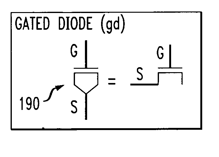
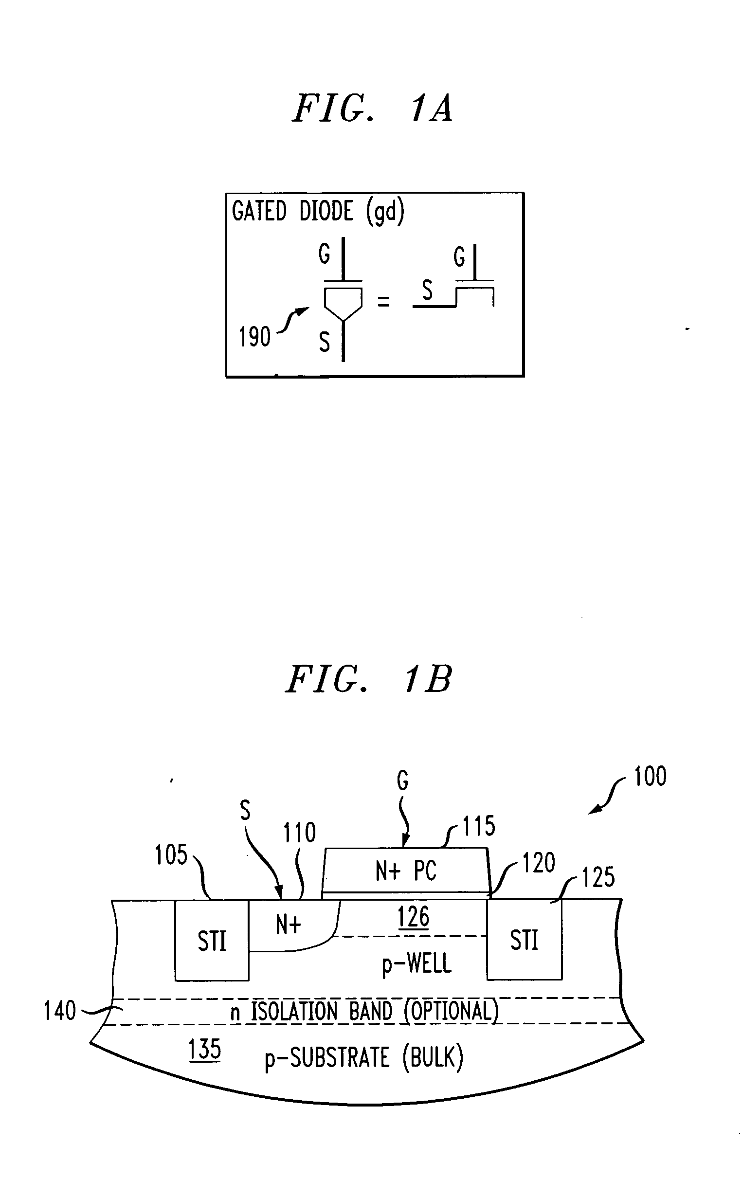
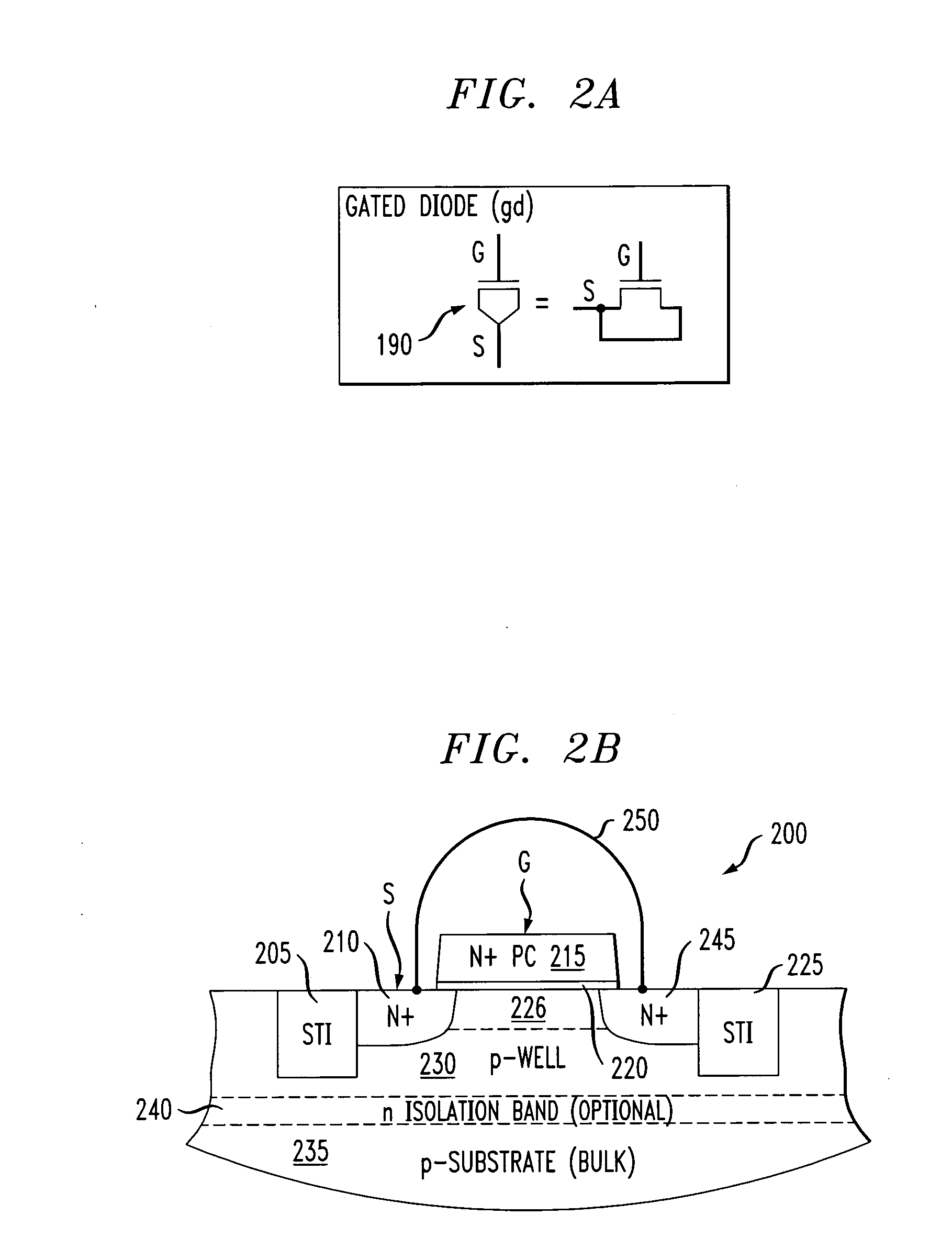
[0049] This disclosure describes high speed, non-destructive read memory cells based on gated diodes, and associated arrays and silicon structures that can be readily implemented in regular logic-based bulk silicon and Silicon-On-Insulator (SOI). The target performance of the memory cells can be comparable to or even better than Static Random Access Memory (SRAM) speed, but can occupy an area 50 to 70 percent of that of SRAM for the same generation of technology. Due to a high gain characteristic of the memory cell itself, the memory can operate at a much lower supply voltage, much less than that required by conventional Dynamic Random Access Memory (DRAM) and SRAM. An important emphasis herein is on the high speed aspects of the memory cells and architecture, with sufficient retention time and low soft error rate in mind.

[0050] For ease of reference, the following disclosure is separated into the following sections: Introduction and Gated Diode Structures; Gated Diode Circuits; 3T...


PUM


Abstract

A memory cell comprises: (1) a write switch, the first terminal of the write switch coupled to an at least one bitline, the control terminal of the write switch coupled to the first control line; (2) a two terminal semiconductor, the first terminal of the two terminal semiconductor device coupled to the second terminal of the write switch, and the second terminal of the two terminal semiconductor device coupled to an at least one second control line, wherein the two terminal semiconductor device has a capacitance when a voltage on the first terminal relative to the second terminal is above a threshold voltage and has a lower capacitance when the voltage on the first terminal relative to the second terminal is less than the threshold voltage; (3) a read select switch, the control terminal of the read select switch coupled to an at least one second control line, the first terminal of the read select switch coupled to the at least one bitline; and (4) a read switch, the control terminal of the read switch coupled to the first terminal of the gated diode and coupled to the second terminal of the write switch, the first terminal of the read switch coupled to the second terminal of the read select gate, and the second terminal of the read switch coupled to ground.

Description

CROSS REFERENCE TO RELATED APPLICATIONS [0001] This application is related to an application by Luk et al., entitled AMPLIFERS USING GATED DIODES, U.S. patent Ser. No. ______, filed on the same day as the present application and assigned to International Business Machines, Inc., the disclosure of which is hereby incorporated by reference.FIELD OF THE INVENTION [0002] The present invention relates to semiconductors and, more particularly, relates to semiconductor memory. BACKGROUND OF THE INVENTION [0003] In the past few decades, Dynamic Random Access Memories (DRAMs) have been delivering higher density but slower speed, and Static Random Access Memories (SRAMs) the higher speed but lower density. These two memory types have been developed separately, following their own technological development curves for density and speed. Recently, embedded memory of DRAM and SRAM began to emerge. Embedded memory is memory on the same “chip” as a processor. Currently, each of DRAM and SRAM also f...

Claims


Application Information

Patent Timeline
IPC IPC(8): G11C11/36H01L21/82G11C11/405G11C11/407H01L27/04H01L27/10H01L27/102H01L27/108H01L29/739
CPCG11C11/405H01L29/7391H01L27/108H01L27/1021H10B12/00H04B1/40
Inventor LUK, WING K.DENNARD, ROBERT H.
Owner GLOBALFOUNDRIES INC
Why Eureka
Try Eureka