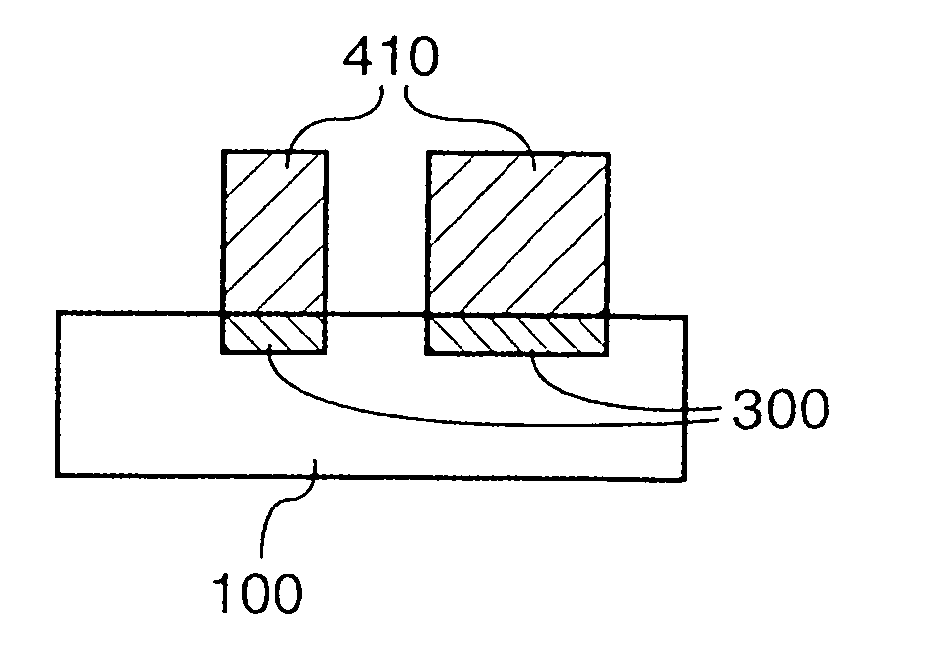
Manufacturing method of monocrystalline gallium nitride localized substrate
a monocrystalline gallium nitride and localization technology, applied in the direction of crystal growth process, polycrystalline material growth, chemically reactive gas, etc., can solve the problems of inability to improve performance, signal delay is inevitable, and limitations in the improvement of performance appear
- Summary
- Abstract
- Description
- Claims
- Application Information
AI Technical Summary
Benefits of technology
Problems solved by technology
Method used
Image
Examples
embodiment 1
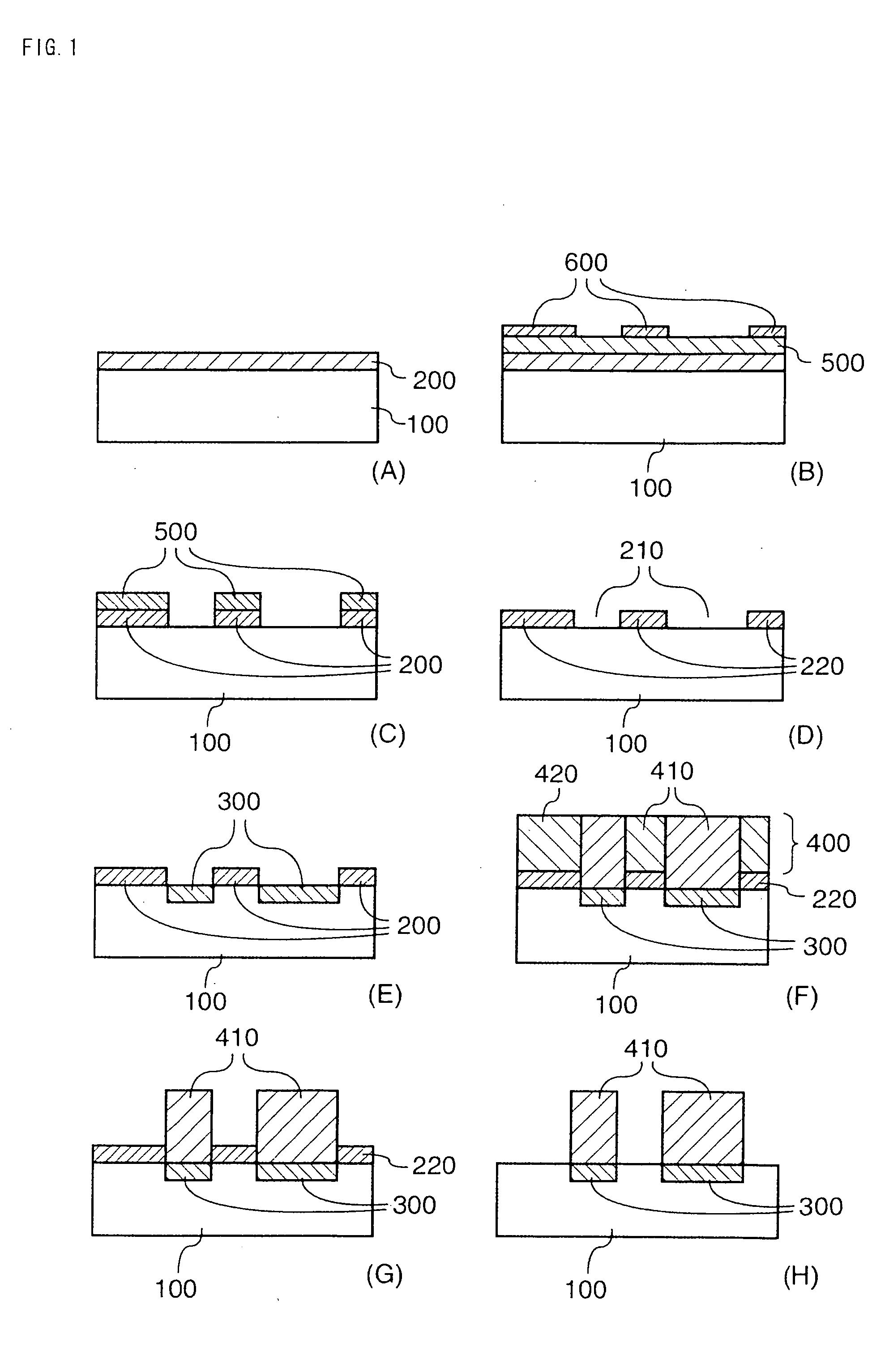
[0015] A monocrystalline gallium nitride localized substrate of the present invention is manufactured in the following manner.
[0016] First, silicon nitride (Si3N4) 200 as a thin film is made to grow by the CVD method on the whole surface of a silicon substrate 100 having a face orientation (111) for film formation (refer to FIG. 1(A)). This silicon nitride 200 functions as a mask in growing gallium nitride 400. That is, the gallium nitride 400 does not grow (does not remain resultingly) in parts in which the silicon nitride 200 is formed.
[0017] Next, a photoresist 500 is applied on the silicon nitride 200 to superpose a photomask 600 thereon in areas in which it is undesirable to grow the gallium nitride 400, and the mask pattern is transferred by the photolithography technique (refer to FIG. 1(B)).
[0018] The silicon nitride 200 in parts of no photoresist 500 is removed by etching with the use of the developed photoresist 500 as a mask (refer to FIG. 1(C)). The developed photores...
embodiment 2
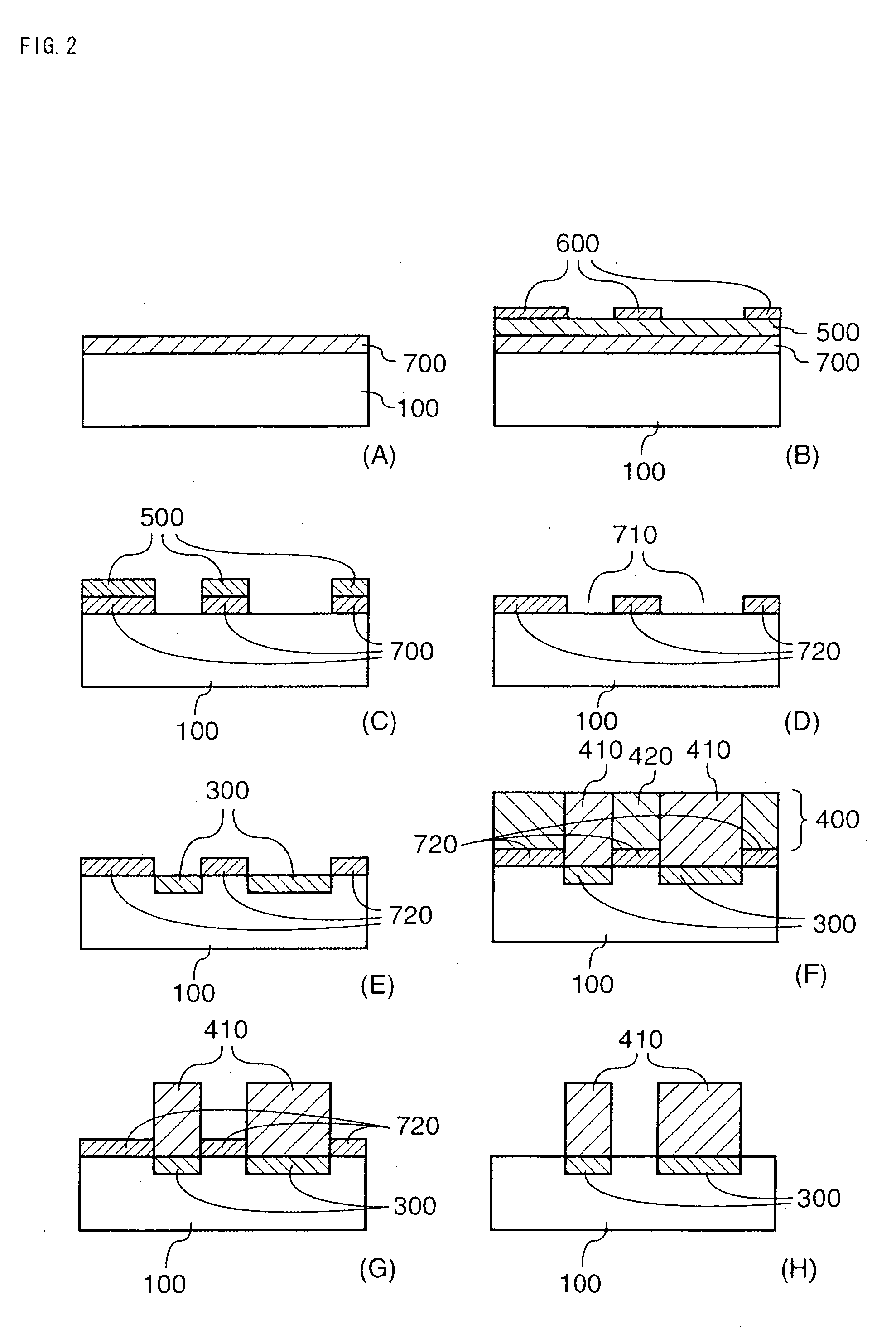
[0025] Secondly, a manufacturing method of a monocrystalline gallium nitride localized substrate of the present invention is described referring to FIG. 2.
[0026] This manufacturing method is as follows. The surface of a silicon substrate 100 having a face orientation (111) for film formation is thermally oxidized to form silicon oxide (SiO2) 700 as a thin film (refer to FIG. 2(A)). This silicon oxide 700 functions as a mask in growing gallium nitride 400. That is, the gallium nitride 400 does not grow (does not remain resultingly) in parts in which the silicon oxide 700 is formed.
[0027] Next, a photoresist 500 is applied on the silicon oxide 700 to superpose a photomask 600 thereon in parts in which it is undesirable to grow the gallium nitride 400, and the mask pattern is transferred by the photolithography technique (refer to FIG. 2(B)).
[0028] The silicon oxide 700 in parts of no photoresist 500 is removed by etching with the use of the developed photoresist 500 as a mask (refe...
PUM
| Property | Measurement | Unit |
|---|---|---|
| temperature | aaaaa | aaaaa |
| speed | aaaaa | aaaaa |
| parasitic capacitance | aaaaa | aaaaa |
Abstract
Description
Claims
Application Information


