Design method for semiconductor integrated circuit suppressing power supply noise

a technology of integrated circuits and power supply noise, applied in the direction of cad circuit design, program control, instruments, etc., can solve the problems of insufficient design margin in relation to power supply fluctuation, inability to analyze power supply noise of semiconductor integrated circuits, and malfunction of transistors, etc., to achieve the effect of suppressing power supply nois

Inactive Publication Date: 2005-07-07
SOCIONEXT INC
View PDF14 Cites 18 Cited by
  • Summary
  • Abstract
  • Description
  • Claims
  • Application Information

AI Technical Summary

Benefits of technology

[0023] Also, by changing a wiring method, the number of pads, or separation of power supplies, a type of package, a characteristic of an inductance element, a substrate structure, a distance between wires, a characteristic of a decoupling capacitance, a length or a width of a wire, or a characteristic of a resistance element, and providing an additional inductance element, decoupling capacitance, or resistance element, it is possible to change an inductance component, a capacitance component, and a resistance component included in an impedance of a power supply wire of a semiconductor integrated circuit, and design a semiconductor integrated circuit suppressing power supply noise.
[0024] Also, by making a design modification in view of an operating frequency band, it is possible to make a design modification in view of pow

Problems solved by technology

If the semiconductor integrated circuit is caused to operate at such a frequency, power supply noise might increase to change the threshold voltage and operating current of a transistor, so that a delay value and an output potential of the transistor are changed, resulting in malfunction of the transistor.
Because of the above reasons, in the semiconductor integrated circuits of recent years, the design margin in relation to power supply fluctuation tends to be insufficient.
However, with conventional transistor-level circuit simulation or substrate noise simulation, it is imp

Method used


Image

  • Design method for semiconductor integrated circuit suppressing power supply noise
  • Design method for semiconductor integrated circuit suppressing power supply noise
  • Design method for semiconductor integrated circuit suppressing power supply noise

Examples


Embodiment Construction

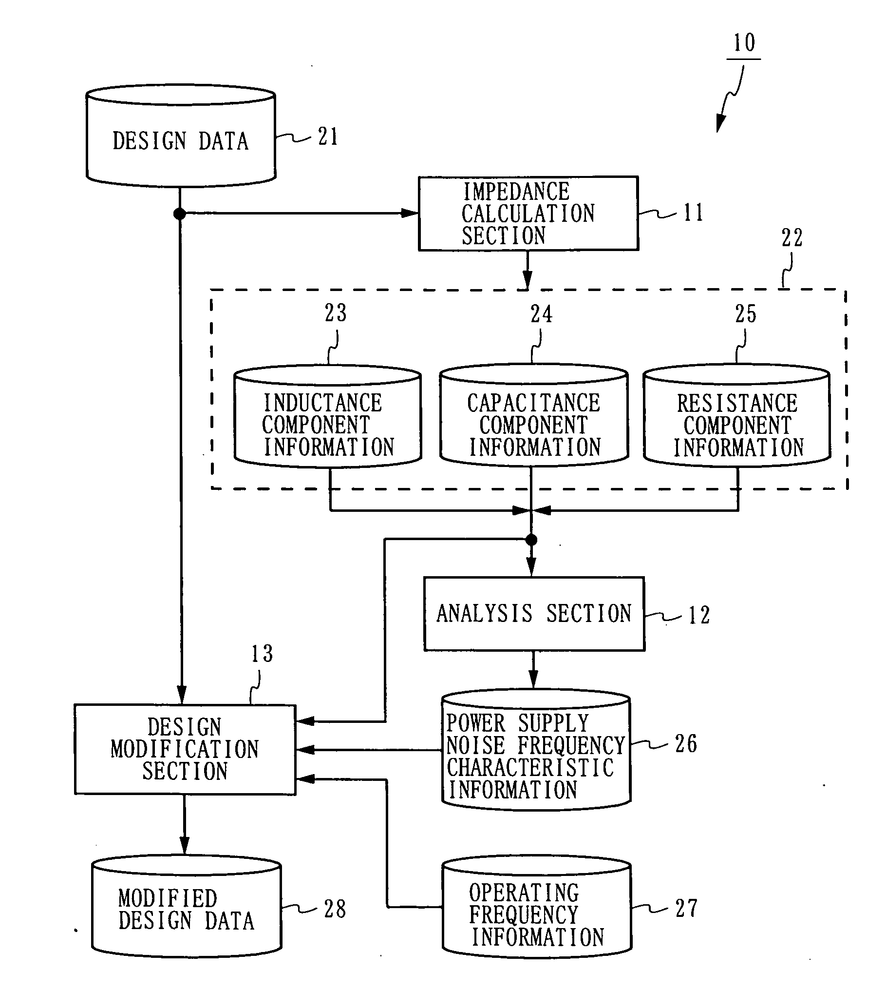
[0040]FIG. 1 is a block diagram showing the structure of a design apparatus executing a design method for a semiconductor integrated circuit according to an embodiment of the present invention. The design apparatus 10 as shown in FIG. 1 includes an impedance calculation section 11, an analysis section 12, and a design modification section 13. Design data 21 and operating frequency information 27 are inputted to the design apparatus 10.

[0041] Roughly speaking, the design apparatus 10 operates as follows. The design data 21 is design data of a semiconductor integrated circuit to be designed (hereinafter, referred to as a target circuit). The operating frequency information 27 indicates a frequency band at which the target circuit operates. The operating frequency information 27 is designated as 200±30 MHz, for example. The impedance calculation section 11 calculates an impedance of the power supply wire of the target circuit based on the design data 21, and outputs the calculation re...


PUM


Abstract

An impedance of a power supply wire is calculated based on design data of a semiconductor integrated circuit, a frequency characteristic of the calculated impedance is obtained, and a design of the semiconductor integrated circuit is changed based on the obtained frequency characteristic. As the above-described impedance, an impedance between power supplies that are different in potential such as a power supply and a ground may be calculated, or an impedance between power supplies that are substantially the same in potential such as a power supply and an N-well power supply may be calculated. By a design modification, a wiring method, the number of pads, separation of power supplies, a type of package, a characteristic of an inductance element, a substrate structure, a distance between wires, a decoupling capacitance, a length of a wire, and a characteristic of a resistance element, for example, are changed.

Description

BACKGROUND OF THE INVENTION [0001] 1. Field of the Invention [0002] The present invention relates to a design method for a semiconductor integrated circuit, and more particularly to a design method for a semiconductor integrated circuit which suppresses power supply noise occurring in a power supply wire. [0003] 2. Description of the Background Art [0004] In order to achieve high-speed operation and low power consumption at the same time, semiconductor integrated circuits of recent years adopt a method for controlling a source power supply (VDD) of a P-channel transistor and a substrate power supply (N-well power supply VSUBN) by separate power supplies, or a method for controlling a source power supply (VSS) of an N-channel transistor and a substrate power supply (P-substrate power supply VSUBP) by separate power supplies. Note that “substrate voltage” as described herein refers to a potential which confronts a potential of a gate, which controls the amount of electric charge in a ...

Claims


Application Information

Patent Timeline
IPC IPC(8): G06F17/50H01L21/82H01L21/822H01L27/04
CPCG06F17/5063G06F17/5036G06F30/36G06F30/367
Inventor SHIMAZAKI, KENJISATO, KAZUHIROICHINOMIYA, TAKAHIROHIRANO, SHOZOTAKAHASHI, MASAOTSUJIKAWA, HIROYUKIKOJIMA, SEIJIRO
Owner SOCIONEXT INC
Why Eureka
Try Eureka