
Semiconductor substrate and semiconductor device using the same

a semiconductor and substrate technology, applied in the direction of semiconductor devices, basic electric elements, electrical equipment, etc., can solve the problems of long current flow path, inability to ensure the desired level of off-stage breakdown voltage necessary for the device,

Inactive Publication Date: 2005-07-14
RENESAS ELECTRONICS CORP
View PDF4 Cites 13 Cited by
  • Summary
  • Abstract
  • Description
  • Claims
  • Application Information

AI Technical Summary

Benefits of technology

The present invention provides a semiconductor substrate with a first layer containing phosphorus and a second layer containing an n-type impurity. A third layer containing an n-type impurity is placed between the first and second layers to prevent phosphorus from diffusing into the second layer. This results in a semiconductor device with a sufficient level of OFF-stage breakdown voltage without the need to increase the thickness of the second layer or increase the ON-stage resistance. The invention allows for a semiconductor substrate that realizes both a high OFF-stage breakdown voltage and a low ON-stage resistance in the fabrication of semiconductor devices with vertical devices.

Problems solved by technology

Phosphorus diffused into the n−-type drift layer 13 may prevent the depletion layer of MOSFET in a product form from fully spreading in the OFF state, and thereby may fail in ensuring a desirable level of OFF-stage breakdown voltage necessary for the device.
This may, however, result in a longer current flow path in a portion having a large specific resistance, and may increase the ON-stage resistance of the vertical device.

Method used


Image

  • Semiconductor substrate and semiconductor device using the same
  • Semiconductor substrate and semiconductor device using the same
  • Semiconductor substrate and semiconductor device using the same

Examples


first embodiment

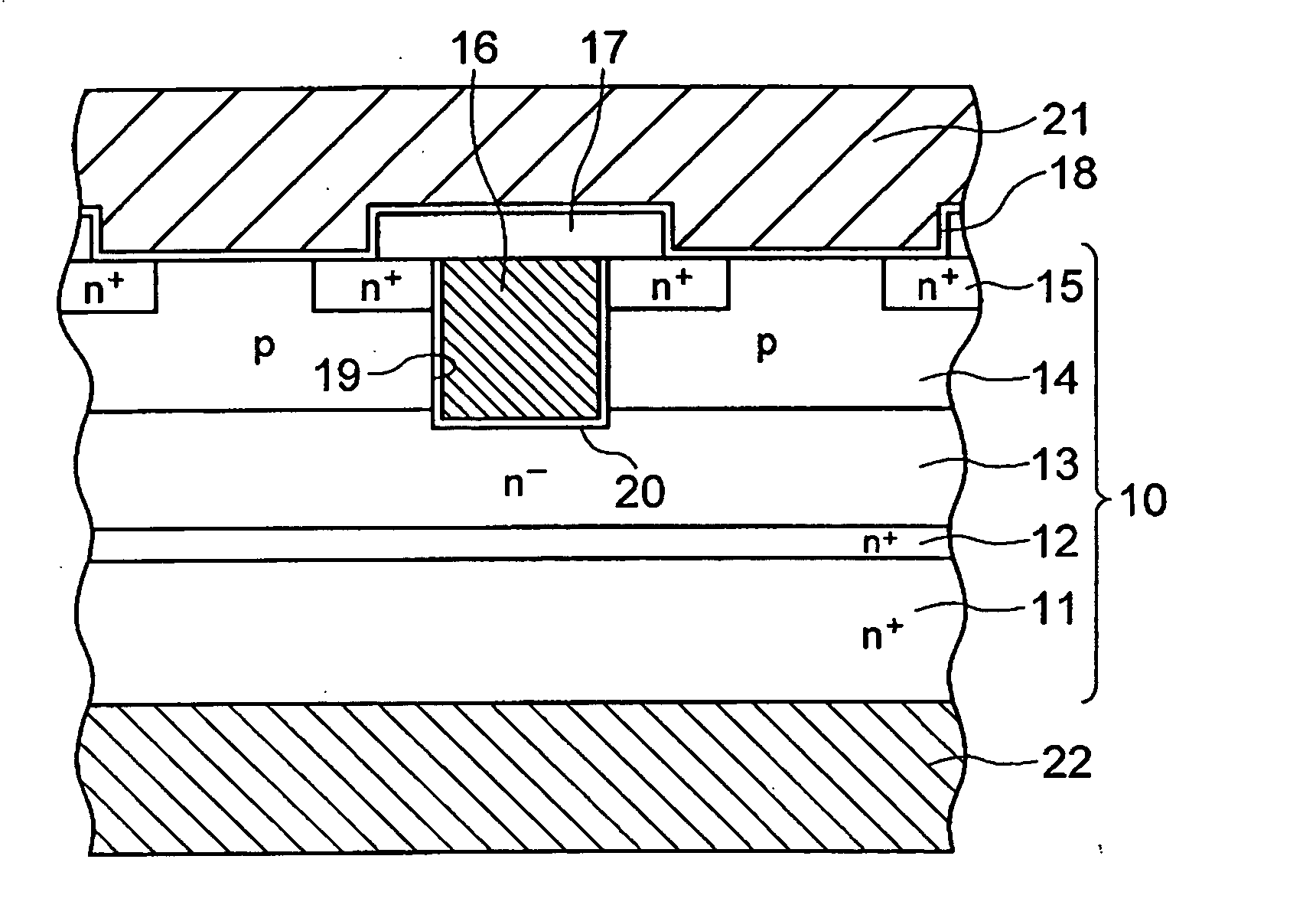
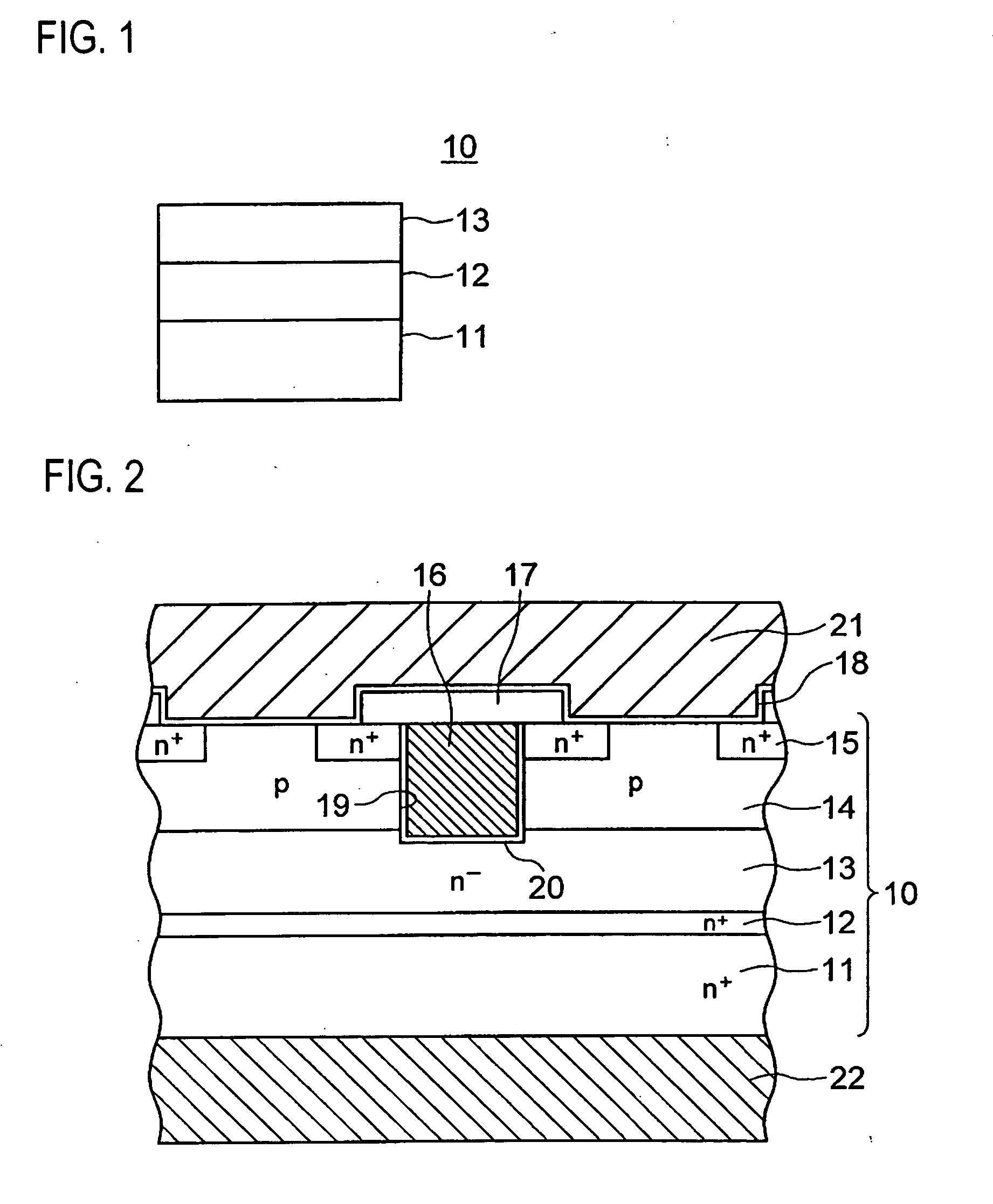
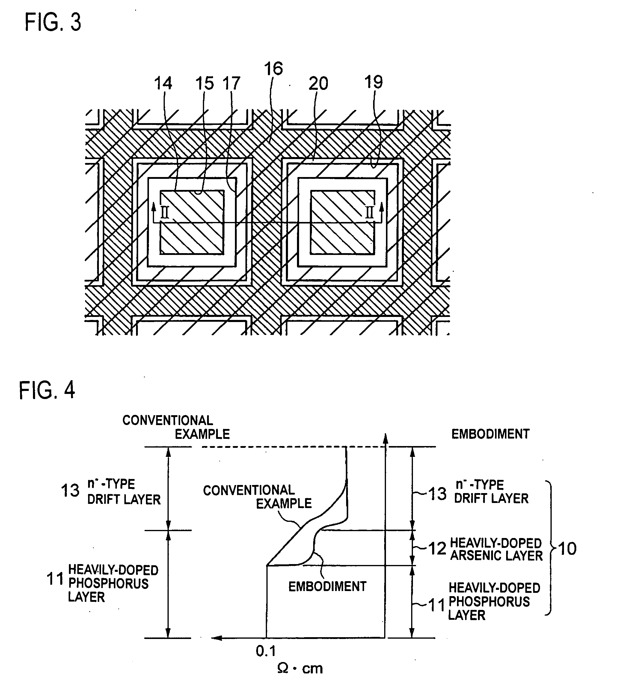
[0036]FIG. 2 and FIG. 3 are sectional view and plan view, respectively, of the semiconductor device according to the present invention, fabricated using the semiconductor substrate shown in FIG. 1. It is to be noted that the upper electrode 21 is not shown in FIG. 3, and FIG. 2 shows a sectional view taken along line II-II in FIG. 3. The semiconductor device of the present embodiment is configured as a semiconductor device having a vertical MOSFET, and, as shown in FIG. 2, has diffusion layers formed in the n−-type drift layer 13 of the semiconductor substrate 10 which comprises the heavily-doped phosphorus layer 11, the heavily-doped arsenic layer 12 and the n−-type drift layer 13.

[0037] In more detail, the vertical MOSFET has the p-type base layer 14 of approximately 1 μm thick formed in the surficial portion of the n−-type drift layer 13 by ion implantation of a p-type impurity, gate electrode 16 of approximately 1 μm deep formed in the p-type base layer 14 so as to reach the n−-...

second embodiment

[0044]FIG. 5 shows a sectional view of a semiconductor device according to the present invention. The semiconductor device of the present embodiment is configured as an insulated gate bipolar transistor (IGBT). In a structural point of view, the IGBT further comprises a p+-type collector layer inserted between the heavily-doped phosphorus layer 11 and lower electrode 22 in the vertical MOSFET shown in FIG. 2. The IGBT has an n+-type, heavily-doped layer 15A, a p-type emitter layer 14A, the n−-type drift layer 13, the heavily-doped arsenic layer 12 and the heavily-doped phosphorus layer 11, and further comprises a base layer connected to a base electrode 16A, and a p+-type collector layer 23, wherein all of these are placed between the upper electrode 21A which composes an emitter electrode and a lower electrode 22A which composes a collector electrode. It is also allowable that the semiconductor substrate having the p-type collector layer 23 can be formed typically by bonding the su...


PUM


Abstract

A semiconductor substrate used for fabricating vertical devices, such as vertical MOSFET, capable of maintaining low ON-stage resistance and of ensuring a necessary level of OFF-stage breakdown voltage is provided. A heavily-doped arsenic layer of 0.5 to 3.0 μm thick is inserted between a heavily-doped phosphorus layer 11 composing the drain of a vertical MOSFET and an n−-type drift layer. The heavily-doped arsenic layer functions as a barrier layer which prevents phosphorus from diffusing from the heavily-doped phosphorus layer into the n−-type drift layer. This is successful in maintaining spreading of the depletion layer during OFF time of the vertical MOSFET to thereby improve the OFF-stage breakdown voltage, and in maintaining the low ON-stage resistance.

Description

[0001] This application is based on Japanese patent application No. 2003-430267 the content of which is incorporated hereinto by reference. DISCLOSURE OF THE INVENTION [0002] 1. Field of the Invention [0003] The present invention relates to a semiconductor substrate and a semiconductor device, and in particular to a semiconductor substrate suitable for fabricating semiconductor devices having vertical devices such as vertical MOSFET, and a semiconductor device fabricated using the semiconductor substrate. [0004] 2. Related Art [0005] Semiconductor devices having vertical devices such as vertical MOSFET and insulated gate bipolar transistor are widely used as high-output semiconductor devices handling high voltage and large current, in the field of power electronics. FIG. 7 shows a conventional vertical semiconductor device described in Japanese Laid-Open Patent Publication No. 2001-7149. The conventional semiconductor device is formed on a semiconductor substrate having a silicon la...

Claims


Application Information

Patent Timeline
Patent Type & Authority Applications(United States)
IPC IPC(8): H01L21/336H01L29/06H01L29/08H01L29/739H01L29/78
CPCH01L29/0696H01L29/0834H01L29/7813H01L29/7397H01L29/7802H01L29/0847H01L29/0878
Inventor OHTANI, KINYA
Owner RENESAS ELECTRONICS CORP
Learn More