Solar cell with epitaxially grown quantum dot material

a quantum dot material and solar cell technology, applied in the field of photovoltaic solar cells, can solve the problems of current limitation of four subcells, imbalance of multijunction cells, and insufficient solar photon absorption of gaas subcells

Active Publication Date: 2005-07-21
CYRIUM TECH INC +1
View PDF13 Cites 210 Cited by
  • Summary
  • Abstract
  • Description
  • Claims
  • Application Information

AI Technical Summary

Benefits of technology

[0084] In addition to defect hardness, other advantages of the invention may be realized. For example, a self-assembled quantum dot material can enhance the conversion efficiency by recovering some of the photon energy that is in excess of the semiconductor bandgap, which would otherwise be lost when photons having higher energies than the effective bandgap impinge on the multifunction solar cell. As is well known, the energy in excess of the effective bandgap can generate phonons. Some of these phonons will be re-absorbed within the quantum dots and be used in thermionic emission processes by raising photocarriers from confined quantum dot states to higher, unconfined, states, before being swept across the depletion region. Hence the higher efficiency.

Problems solved by technology

This clearly leads to a current imbalance in the multijunction cell.
Relatively speaking, the GaAs subcell does not absorb enough solar photons while the Ge subcell captures too many.
However, this four-subcell arrangement is still current-limited by the GaAs subcell.
In this scenario, the second subcell absorbs more photons having energies greater than that of its bandgap thus leading to more thermally wasted energy.
This compromises the spatial density of the material that can be used to absorb light and is likely to require thicker layers to absorb the same number of photons as would be absorbed in uniform layers or, larger surfaces which would reduce the conversion efficiency.

Method used


Image

  • Solar cell with epitaxially grown quantum dot material
  • Solar cell with epitaxially grown quantum dot material
  • Solar cell with epitaxially grown quantum dot material

Examples


first embodiment

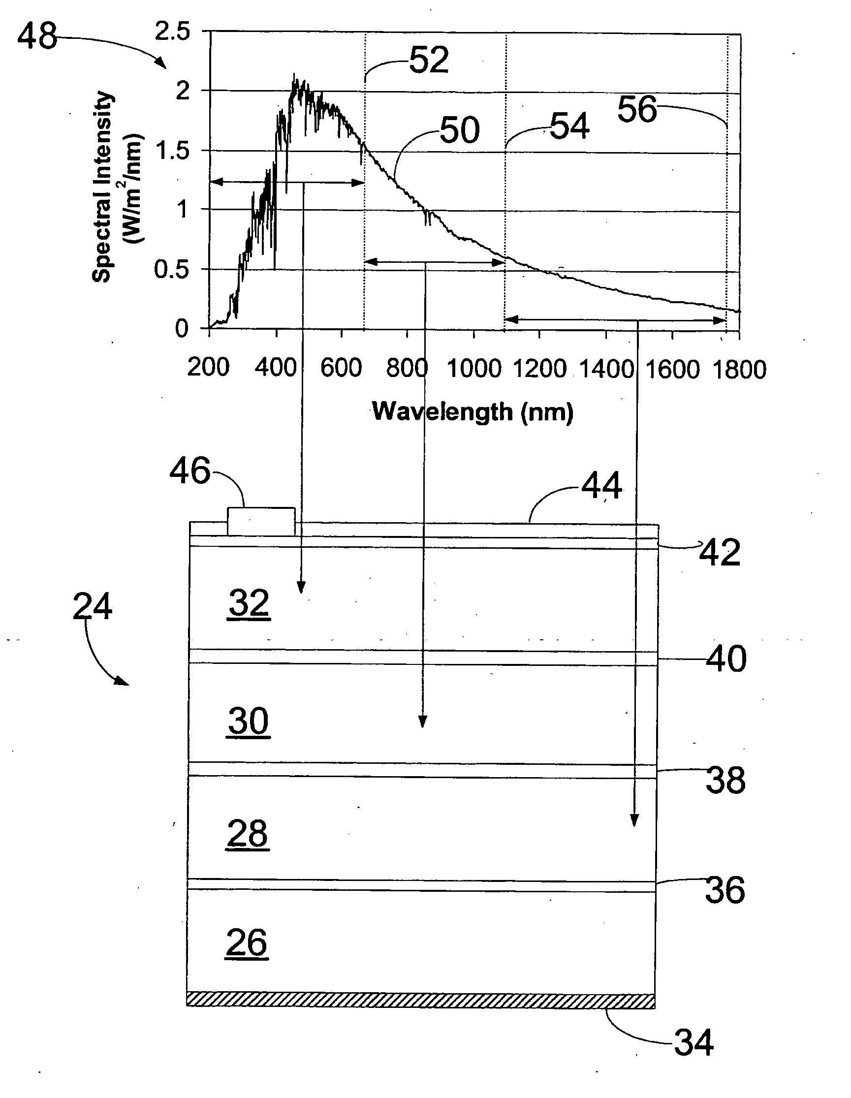
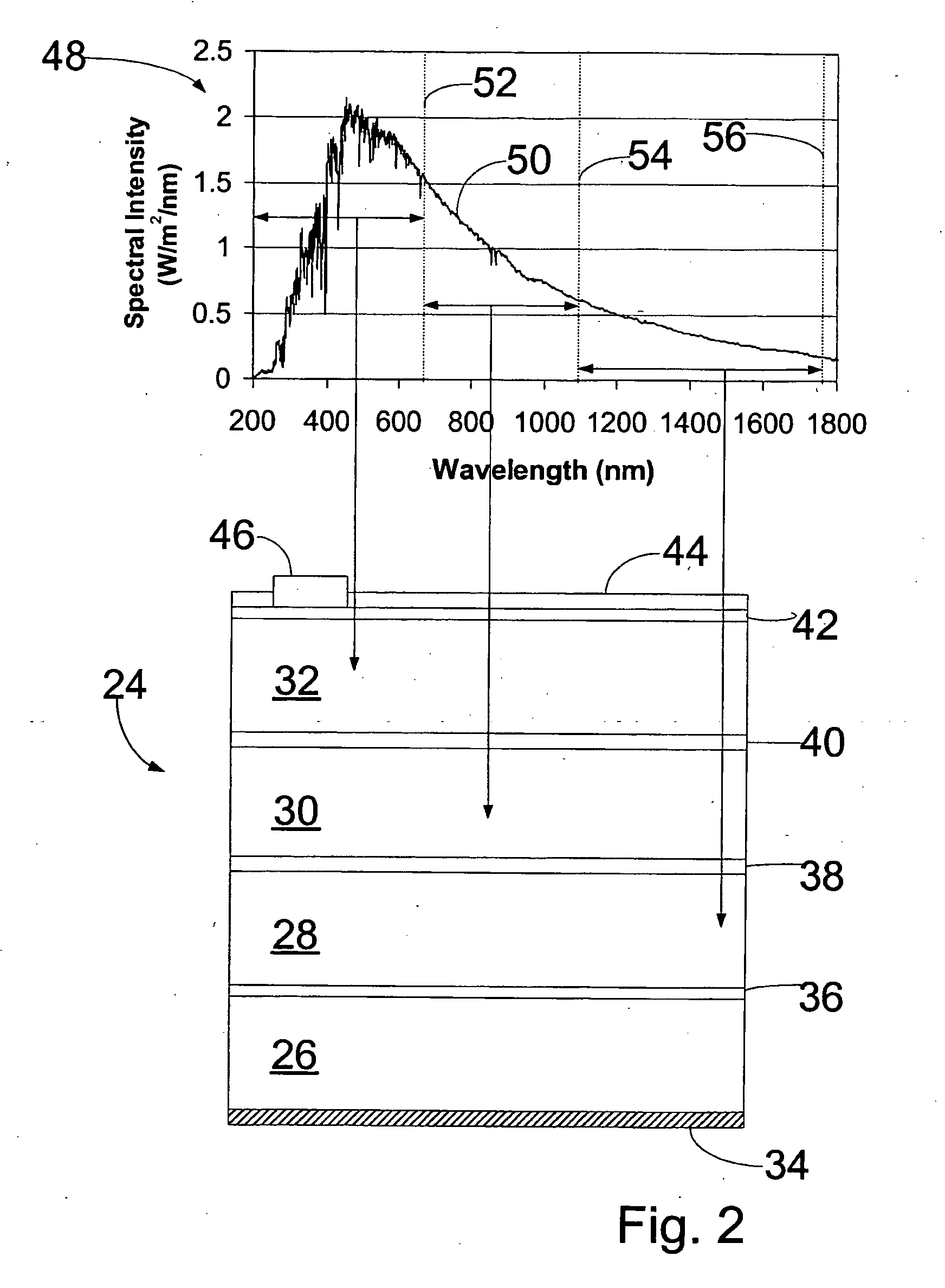
[0033] The first embodiment is a high efficiency monolithic three-junction photovoltaic solar cell. Three-junction photovoltaic solar cells can be fabricated by stacking p-n or n-p junctions made of different semiconductor materials. As stated above, conversion efficiencies of approximately 30% have been obtained using a Ge bottom subcell grown on a Ge substrate, with a GaAs middle subcell and a GaInP or AlGaAs top subcell. The efficiency of such a multijunction photovoltaic solar cell is improved in the present invention by using self-assembled quantum dot material in the middle subcell instead of bulk GaAs.

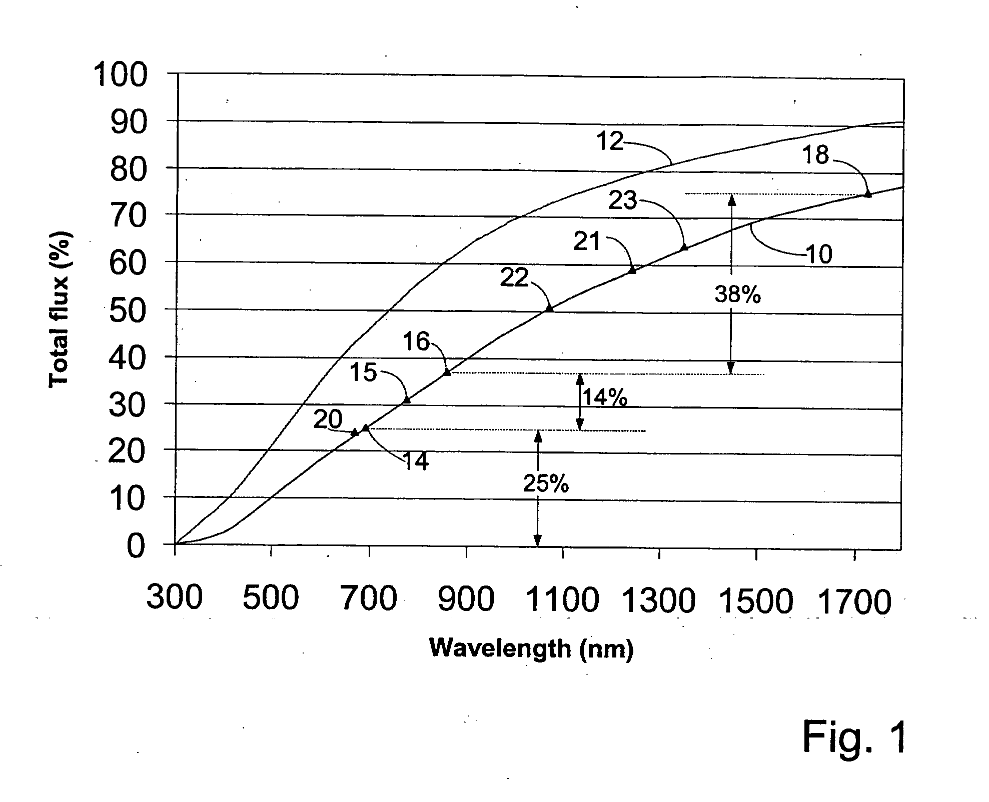
[0034] The principle of the invention is illustrated in FIG. 1 where plot 10 shows the percentage of the AM0 solar photon flux, integrated from the 200 nm wavelength, as a function of wavelength, and plot 12 shows the percentage of the AM0 solar power flux integrated from 200 nm wavelength as a function of wavelength. Reference numerals on plot 10 indicate semiconductor material...

second embodiment

[0056] the invention provides high efficiency monolithic four-junction photovoltaic solar cells. Self-assembled quantum dot material 94 may be adapted to absorb photons with energies greater than about 1.0 eV, indicated as material 21 in FIG. 1. Such a material can be used to fabricate a high-efficiency monolithic four-junction photovoltaic solar cell depicted in FIG. 5 where the subcells will be current-matched if each of the subcells absorbs about 19% of the solar flux.

[0057] The four-junction solar cell comprises substrate 108 upon which first subcell 110 is fabricated. First subcell 110 preferably includes germanium with an appropriate doping profile, the germanium being grown on substrate 108 by epitaxy or by other crystal growth methods. Alternatively, first subcell 110 can be fabricated by intermixing or implanting dopants in bulk germanium material such as, for example, a Ge substrate to create the appropriate doping profile. For example, when III-V semiconductor materials a...

third embodiment

[0069] the invention provides high efficiency monolithic dual-junction photovoltaic solar cells. In another embodiment, a self-assembled quantum dot material is adapted to be used in a dual-junction solar cell. In order to have a high efficiency photovoltaic dual-junction solar cell, a first subcell having a self-assembled quantum dot material similar to self-assembled quantum dot material 94, but with an absorption edge at 0.92 eV, is required together with a second subcell having a material absorbing photons with energies greater than about 1.6 eV. The second subcell may also include a self-assembled quantum material similar to self-assembled quantum dot material 94. Such a dual-junction solar cell would have balanced currents generated in each subcell. Furthermore, each subcell would absorb about 31% of the total solar photon flux, as shown on plot 10 in FIG. 1 where bandgap 15 (1.6 eV) and bandgap 23 (0.92 eV) are depicted.

[0070] A dual-junction photovoltaic solar cell of the pr...


PUM


Abstract

A monolithic semiconductor photovoltaic solar cell comprising a plurality of subcells disposed in series on an electrically conductive substrate. At least one subcell of the plurality of subcells includes an epitaxially grown self-assembled quantum dot material. The subcells are electrically connected via tunnel junctions. Each of the subcells has an effective bandgap energy. The subcells are disposed in order of increasing effective bangap energy, with the subcell having the lowest effective bandgap energy being closest to the substrate. In certain cases, each subcell is designed to absorb a substantially same amount of solar photons.

Description

CROSS REFERENCE TO RELATED APPLICATIONS [0001] This application claims the benefit of U.S. Provisional Application No. 60 / 537,259, filed Jan. 20, 2004, which is incorporated herein by reference.FIELD OF THE INVENTION [0002] The present invention relates generally to photovoltaic solar cells. More particularly, the invention relates to III-V multijunction semiconductor solar cells having an epitaxially grown quantum dot material. BACKGROUND OF THE INVENTION [0003] The sun emits a wide optical spectrum that peaks in the visible and has 60% of its photon flux in the wavelength range spanning from ˜350 nm to ˜1350 nm. This wavelength range corresponds to 80% of the sun's total power flux of ˜1.3 kW / M2 at the earth. [0004] It has been known for decades that the best approach to convert the sun's optical power into electrical power is through solar cells that make use of absorption transitions in semiconductors. Photon energy is harnessed in this way by exciting electrons from the semicon...

Claims


Application Information

Patent Timeline
Patent Type & Authority Applications(United States)
IPC IPC(8): H01L31/00H01L31/042H01L31/18
CPCB82Y10/00B82Y20/00Y02E10/544H01L31/0687H01L31/035236Y02E10/547
Inventor FAFARD, SIMON
Owner CYRIUM TECH INC
Why Eureka
Try Eureka