Capacitor, semiconductor device, and manufacturing method thereof

Inactive Publication Date: 2005-07-21
SEMICON ENERGY LAB CO LTD
View PDF74 Cites 23 Cited by
  • Summary
  • Abstract
  • Description
  • Claims
  • Application Information

AI Technical Summary

Benefits of technology

[0024] As described in the above, according to the present invention, first, in order to prevent short circuit due to a pin hole formed accidentally in the dielectric of the storage capacitor, the pin hole is filled up with the insulating material to prevent defects due to formation of the storage capacitor. Further, by forming the spacer of the insulating film made of the resin material, the device is prevented from being broken due

Problems solved by technology

However, since the stored capacitance of the capacitors gradually decreases due to leakage current caused by, for example, OFF current of the pixel TFTs (drain current which exists in spite of the OFF state of the TFTs), the light transmission amount varies to decrease the contrast in image display.
However, there is a fear that the storage capaci

Method used


Image

  • Capacitor, semiconductor device, and manufacturing method thereof
  • Capacitor, semiconductor device, and manufacturing method thereof
  • Capacitor, semiconductor device, and manufacturing method thereof

Examples


Example

Embodiment 1

[0054] An embodiment according to the present invention is described by using FIGS. 5A to 8B. A method for fabricating at the same time, TFTs for a pixel portion and a driver circuit provided in its peripheral, is described here. Note that a CMOS circuit which is a basic circuit for a shift register and buffer etc., and an n-channel TFT forming a sampling circuit (transfer gate) are shown for the driver circuit for the simplicity of explanation.

[0055] In FIG. 5A, it is preferable to use a glass substrate or a quartz substrate for substrate 501. Other than those, a silicon substrate, a metal substrate or a stainless steel substrate having an insulating film formed on the surface thereof may be used. If heat resistivity permits, it is also possible to use a plastic substrate.

[0056] A base film 502 which comprises an insulating film comprising silicon (“an insulating film comprising silicon” generically represents a silicon oxide film, a silicon nitride film and a silico...

Example

Embodiment 2

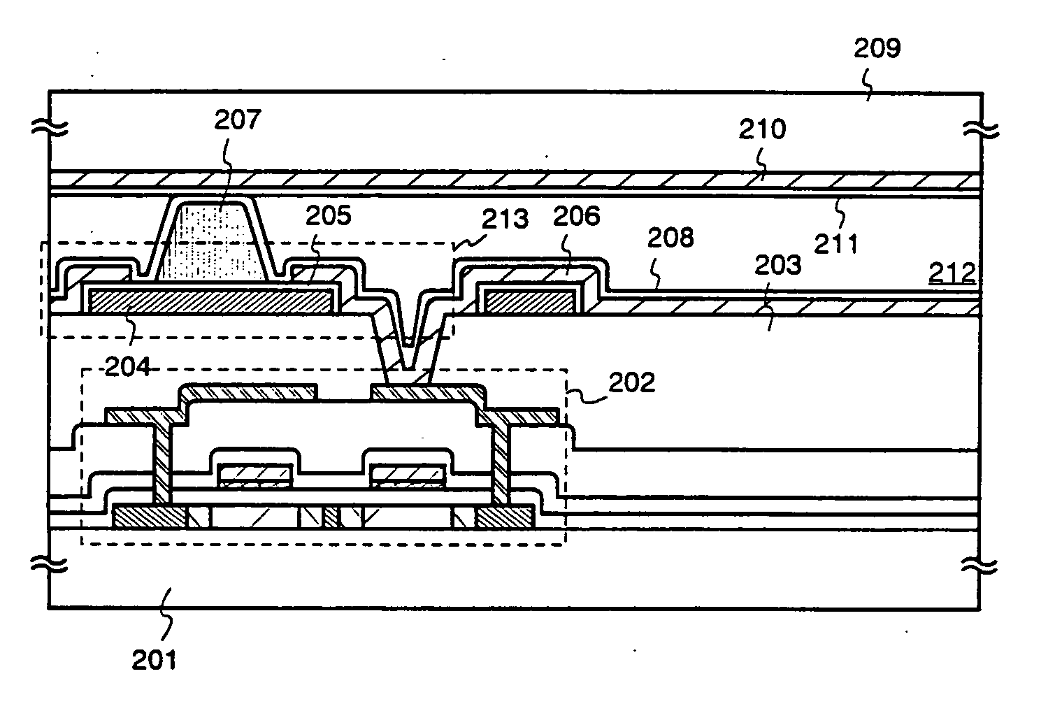
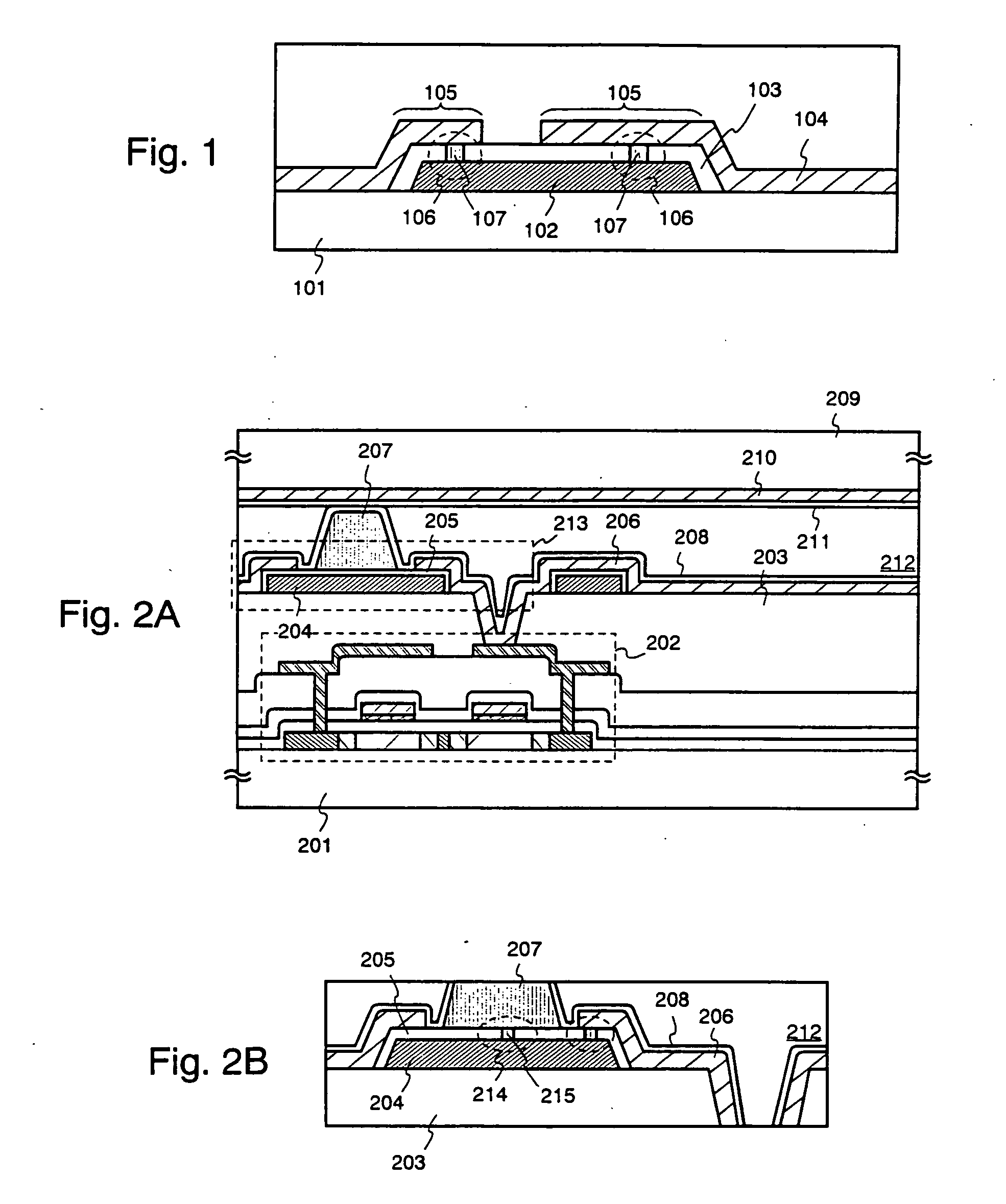
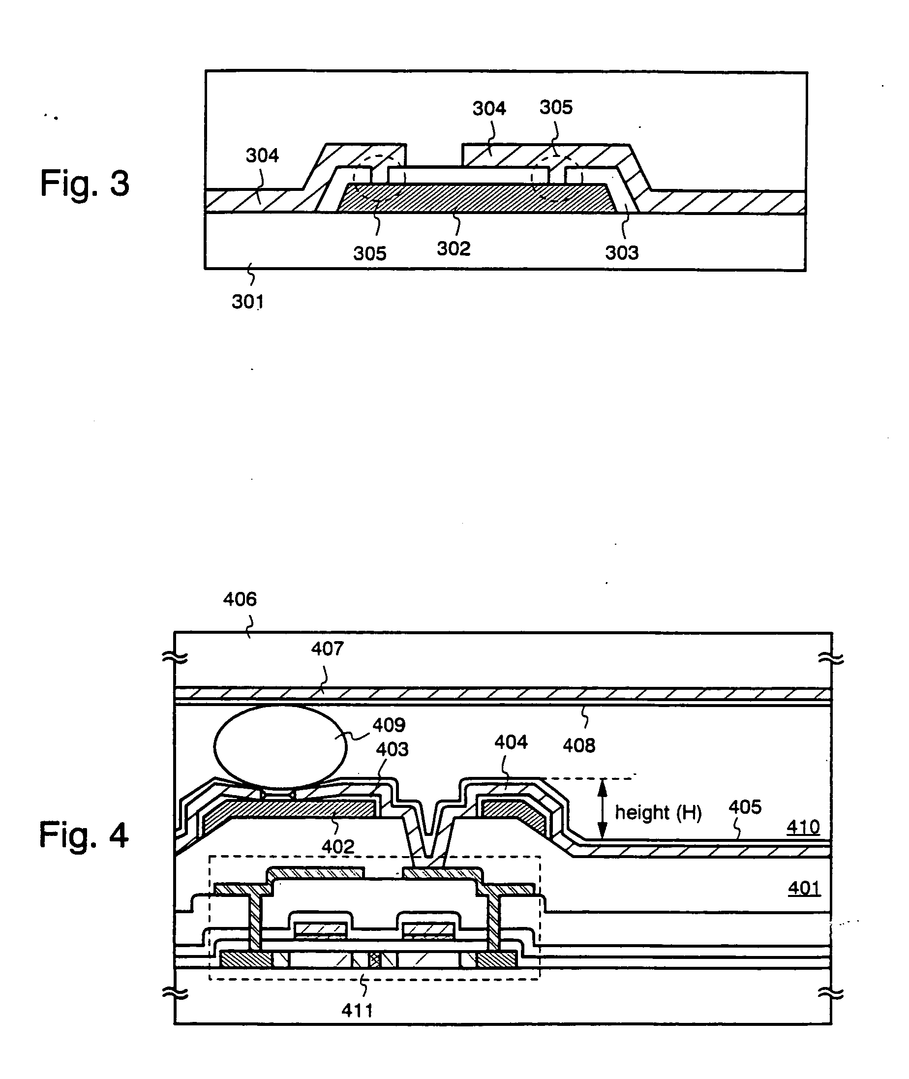
[0148] In the present embodiment, the structure of the active matrix liquid crystal display device in Embodiment 1 is described with reference to the perspective view of FIG. 10. An active matrix substrate is formed of a pixel portion 802, a driver circuit 803 on the gate side, and a driver circuit 804 on the source side formed on a glass substrate 801. A pixel TFT 805 in the pixel portion (which corresponds to the pixel TFT 704 shown in FIG. 8B) is an n-channel TFT, and is connected with a pixel electrode 806 and a storage capacitor 807 (which corresponds to the storage capacitor 572 shown in FIG. 8A).

[0149] The driver circuits provided on the periphery are formed based on a CMOS circuit. The driver circuit 803 on the gate side and the driver circuit 804 on the source side are connected with the pixel portion 802 through a gate wiring 808 and a source wiring 809, respectively. An external input / output terminal 811 connected with an FPC 810 is provided with input / outpu...

Example

Embodiment 3

[0151]FIG. 11 shows an example of circuit structure of the active matrix substrate shown in embodiment 2. The liquid crystal display device of embodiment 3 comprises a source side driver circuit 901, a gate side driver circuit (A) 907, a gate side driver circuit (B) 911, a pre-charge circuit 912 and a pixel portion 906. Through the Specification, driver circuit is a generic name including a source side processing circuit and a gate side driver circuit.

[0152] The source side driver circuit 901 is provided with a shift register 902, a level shifter 903, a buffer circuit 904, and a sampling circuit 905. Further, the gate side driver circuit (A) 907 is provided with a shift register 908, a level shifter 909, and a buffer circuit 910. The scanning signal driver circuit (B) 911 has a similar structure.

[0153] The driver voltages for the shift register 902 and 908 is between 5 and 16 V here (typically 10 V), and the structure shown by reference numeral 702 in FIG. 8B is suita...


PUM


Abstract

A highly reliable capacitor, a semiconductor device having high operating performance and reliability, and a manufacturing method thereof are provided. A capacitor formed of a first conductive film 102, a dielectric 103 made of an insulating material, and a second conductive film 104 is characterized in that a pin hole 106 formed by chance in the dielectric 103 is filled up with an insulating material (filler) 107 made of a resin material. This can prevent short circuit between the first conductive film 102 and the second conductive film 104. The capacitor is used as a storage capacitor provided in a pixel of a semiconductor device.

Description

BACKGROUND OF THE INVENTION [0001] 1. Field of the Invention [0002] The present invention relates to a semiconductor device having a circuit formed of a thin film transistor (hereinafter referred to as a TFT) on an insulator (substrate) having an insulating surface, and to a manufacturing method thereof. In particular, the present invention relates to an electro-optical device represented by a liquid crystal display device where a pixel portion and a driver circuit provided on the periphery thereof are provided on the same insulator, and to an electric apparatus (electronic device) having such an electro-optical device mounted thereon. It is to be noted that a semiconductor device as used herein means any device which functions by utilizing semiconductive characteristics, and the above-mentioned electro-optical device and electric apparatus having the electro-optical device mounted thereon are included in semiconductor devices. [0003] 2. Description of the Related Art [0004] Develop...

Claims


Application Information

Patent Timeline
IPC IPC(8): G02F1/1339G02F1/136G02F1/1368H01L21/02H01L21/20H01L21/265H01L21/336H01L21/77H01L21/822H01L27/04H01L27/108H01L27/13H01L29/786
CPCH01L28/40H01L29/78633H01L27/1255H01L29/78645H01L29/78636G02F1/13392G02F1/136213G02F1/136227H01L27/1214H01L27/13
Inventor MURAKAMI, SATOSHIHIRAKATA, YOSHIHARUFUJIMOTO, ETSUKOYAMAZAKI, YUYAMAZAKI, SHUNPEI
Owner SEMICON ENERGY LAB CO LTD
Why Eureka
Try Eureka