
Semiconductor memory device

a memory device and semiconductor technology, applied in the field of single intersection type (open bit line type) semiconductor memory devices, can solve the problems of insufficient stability of plate potentials, interference noise that is not negligible on the plate electrode, and dominant noise between adjacent bit lines, so as to reduce the relative variation between the pair transistors and increase the operation stability of the sense amplifier circui

Inactive Publication Date: 2005-07-21
CETUS TECH INC
View PDF14 Cites 10 Cited by
  • Summary
  • Abstract
  • Description
  • Claims
  • Application Information

AI Technical Summary

Benefits of technology

"The present invention provides a semiconductor memory device with improved operation margin by suppressing interference noise between bit lines and plate electrodes. The invention achieves this by disclosing shielding wires between bit lines and forming common wiring layers for the plate electrodes of dynamic memory cells. Additionally, the invention provides a layout configuration for the dynamic memory cells in dynamic RAMs using planer memory cells to achieve high integration and stable operations. The invention also includes a plurality of global bit lines and plate electrode potential-supplying lines to further reduce interference noise and improve data read operation."

Problems solved by technology

However, as the present inventors studied the noise interference in single intersection type dynamic RAMs, it has been found that interference noise between adjacent bit lines is dominant among the noise interference concerning recent microfabrication processes and that there is noise that is not negligible on the plate electrodes.
To reduce the plate noise, it is insufficient to stabilize plate potentials using the techniques disclosed in the foregoing first and second publications.
Moreover, no suggestions are made for the interference noise between adjacent bit lines.
Furthermore, both techniques in the publications require an additional step of forming the plate electrodes in addition to the step of forming the gate electrodes of transistors, and therefore, they have drawbacks of many fabrication steps and increased wafer cost.
When amplifying operation is performed by the sense amplifier under this state, it is often the case that data are erroneously amplified if the sense amplifier is off-balance because the read margin for the high level is small in the bit line BL1.
Because these noises further delay the amplifying speed of the complementary bit line pair (BL1, NBL1), the data of the complementary bit line pair (BL1, NBL1) are inverted, resulting in a read error.
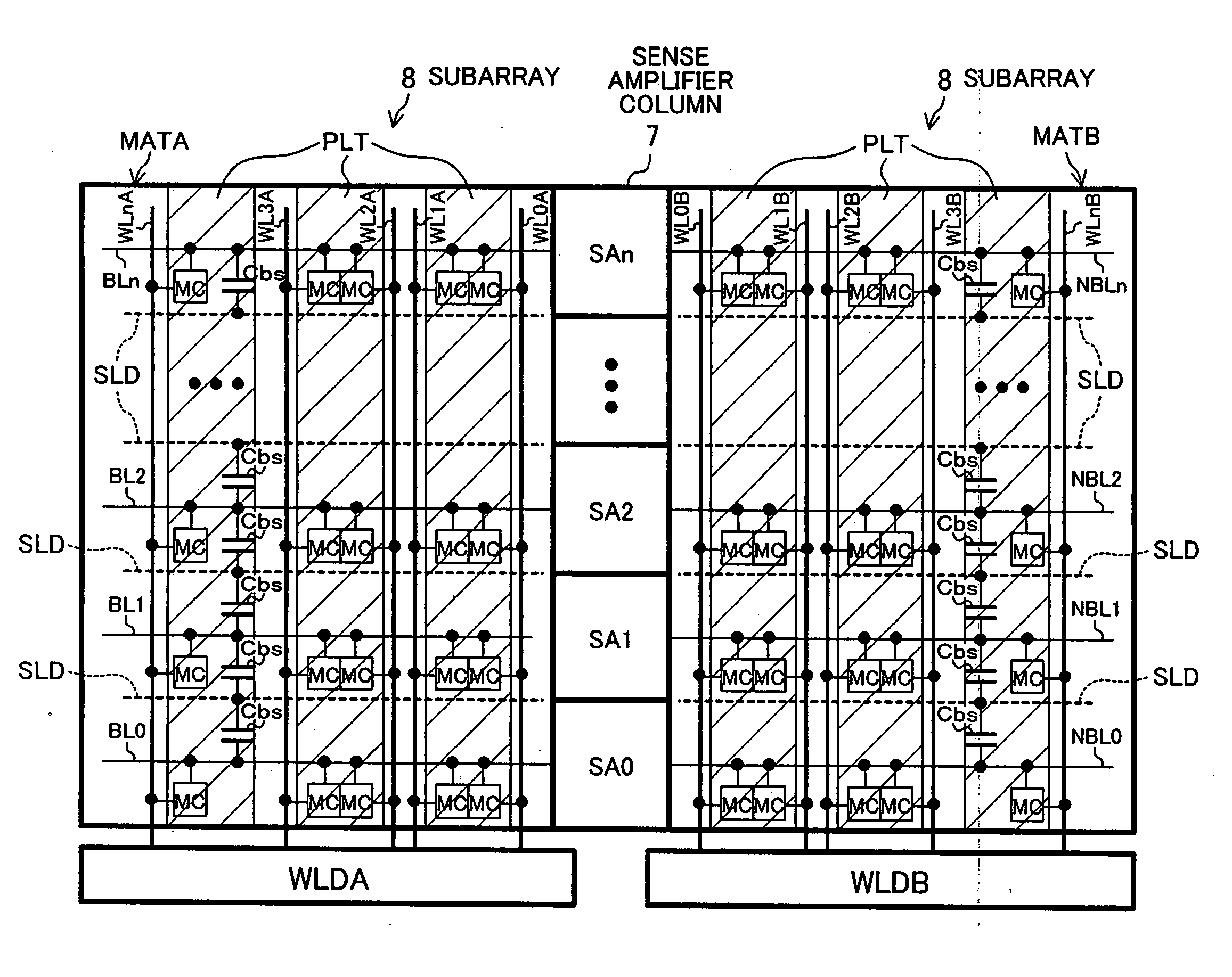
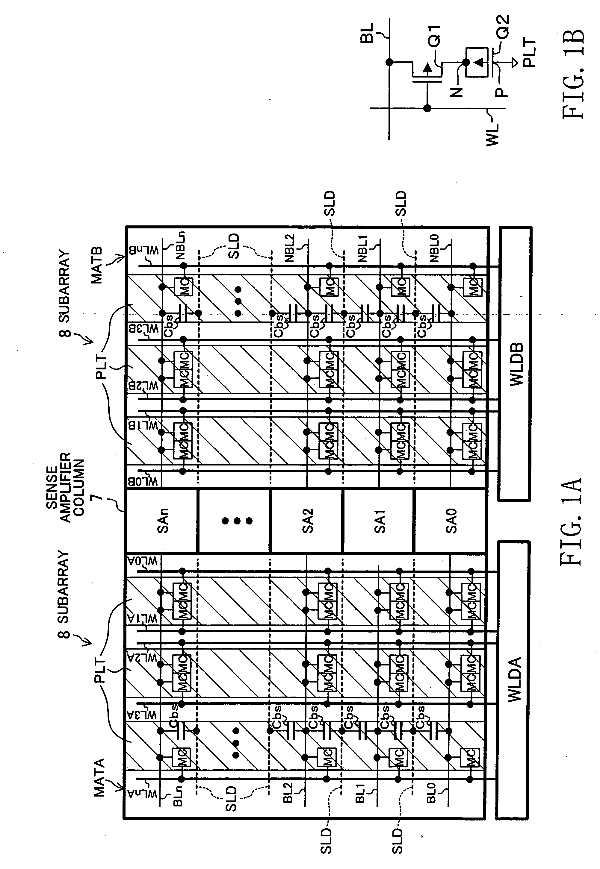
Thus, in single intersection type memory arrays, there is a possibility of read errors depending on data patterns read out to the bit lines because parasitic capacitance exists between adjacent bit lines.
In particular, when the amount of signal charge stored in a memory cell reduces due to leak current or the like, the signal level read out to the bit line further reduces, further increasing the possibility of read errors.
In addition, if they have large operational variations between N-channel and P-channel pair transistors constituting the sense amplifier circuits, their operations are not stable and there is a possibility of data read errors.

Method used


Image

  • Semiconductor memory device
  • Semiconductor memory device
  • Semiconductor memory device

Examples


embodiment 1

[0052]FIG. 14 schematically shows the whole layout of a semiconductor memory device according to Embodiment 1 of the present invention.

[0053] The figure shows a memory chip 10 that constitutes a dynamic RAM. In this memory chip 10, reference numerals 1 represents a memory control circuit block disposed on the left end in the figure, numeral 2 represents a read and write amplifier and a column-selecting circuit block disposed on the right of the memory control circuit block in the figure, numeral 3 represents a row decoder and word line-driving circuit block disposed in the center and along the longitudinal direction of the memory chip 10, numeral 4 represents an internal power-generating circuit block disposed on the right end in the figure, and numeral 5 represents two memory blocks separately disposed above and below the row decoder and word line-driving circuit block 3.

[0054] The memory block 5 has memory arrays 6 that are disposed so that each row along the longitudinal direct...

embodiment 2

[0092] A semiconductor memory device according to Embodiment 2 of the invention is described below. The present embodiment relates to an improvement of the layout configuration of sense amplifier circuits and bit lines in a dynamic RAM.

[0093] Before detailing the present embodiment, the layout configuration shown in FIG. 9 is described. In the figure, BL0, BL1, NBL0, and NBL1 denote respective bit lines; the bit lines BL0 and NBL0 constitute a complementary bit line pair, and the bit lines BL1 and NBL1 constitute another complementary bit line pair. The bit lines BL0, BL1, NBL0, and NBL1 are formed in the same metal wiring layer (a first metal wiring layer), both in the regions of the subarrays 8 and in the region of the sense amplifier.

[0094] NSA0, NSA1, PSA0, and PSA1 denote pair transistors that form respective pairs in the sense amplifier circuit (CMOS latch circuit). In the bit line pairs (BL0, NBL0) and (BL1, NBL1), ones of the bit lines BL0 and BL1 and the other ones of the...

embodiment 3

[0107] Next, another example of the present invention is described with referent to FIG. 13. The present embodiment pertains to an improvement of a latch circuit in the sense amplifier circuit.

[0108] First, a conventional configuration is described. FIG. 12 is a schematic view of a conventional layout configuration of pair transistors that constitute a latch circuit in a sense amplifier circuit. In the figure, OD denotes an active region, Q1 and Q2 denote pair transistors that form a pair in the latch circuit, BL and NBL denote a pair of complementary bit lines, and S denotes a common source of the pair transistors Q1 and Q2. One of the bit lines BL is connected to the gate of one of the transistors Q1 and the drain of the other transistor Q2, and the other bit line NBL is connected to the gate of the other transistor Q2 and the drain of the one of the transistors Q1. The gate electrodes G1 and G2 of the respective pair transistors Q1 and Q2 are disposed parallel to each other in t...


PUM


Abstract

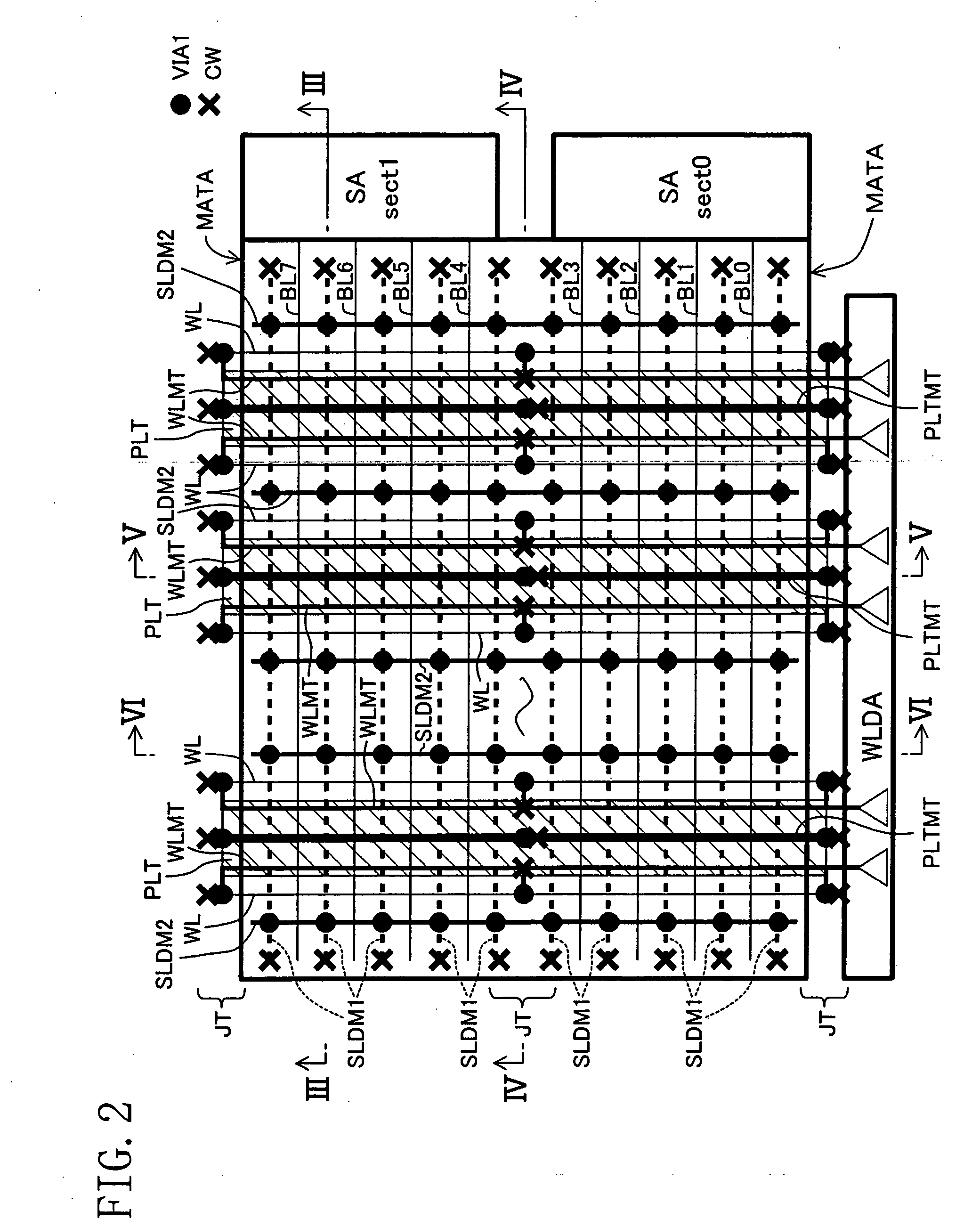
In a single intersection type (open bit line type) dynamic RAM, sub-arrays are disposed to the left and right sides of a sense amplifier column placed at the center. Each sub-array has a multiplicity of dynamic memory cells. In the subarrays located to the left and right of the sense amplifier column, bit lines in the same row constitute a complementary bit line pair. In each subarray, shielding wiring patterns that are formed parallel to, and in the same wiring layer of, these bit lines are disposed between the bit lines. All of these wiring patterns are set at a fixed potential, such as a power supply potential. Thus, interference noise between adjacent bit lines is effectively reduced.

Description

BACKGROUND OF THE INVENTION [0001] The present invention relates to semiconductor memory devices, such as random access memories, and more particularly to a single intersection type (open bit line type) semiconductor memory device in which bit lines connected to dynamic memory cells extends to the left and right of a sense amplifier column placed at the center. [0002] Japanese Unexamined Patent Publication Nos. 59-2365 and 2001-118999 are examples of conventional semiconductor memory devices. The techniques disclosed in these publications pertain to a single intersection type (open bit line type) dynamic RAM that comprises dynamic memory cells each having a transistor and a capacitor, word lines, and bit lines, and that two bit lines constituting a complimentary bit line pair extend to the left and right of a sense amplifier column placed at the center. [0003] The first one of the publications aims at avoiding that, in the case of using an information-storing capacitor utilizing a M...

Claims


Application Information

Patent Timeline
Patent Type & Authority Applications(United States)
IPC IPC(8): G11C11/401G11C7/18G11C11/409H01L21/3205H01L21/82H01L23/52H01L23/522H01L27/04H10B12/00
CPCG11C7/02G11C7/18H01L23/5225H01L27/10882H01L27/10885H01L2924/0002H01L27/10897H01L2924/3011H01L2924/00H10B12/48H10B12/482H10B12/50H01L27/04
Inventor HIROSE, MASANOBUIIDA, MASAHISAOHTA, KIYOTO
Owner CETUS TECH INC
Learn More