Group III Nitride Crystal Substrate, Method of Its Manufacture, and Group-III Nitride Semiconductor Device

a nitride crystal and substrate technology, applied in the direction of crystal growth process, polycrystalline material growth, chemically reactive gas, etc., can solve the problems of low crystal surface planarity, slow crystal growth, low dislocation density, etc., and achieve low dislocation density and low cost.

Active Publication Date: 2005-07-28
SUMITOMO ELECTRIC IND LTD
View PDF9 Cites 24 Cited by
  • Summary
  • Abstract
  • Description
  • Claims
  • Application Information

AI Technical Summary

Benefits of technology

[0021] In accordance with the present invention, Group-III nitride crystal substrates that are of low dislocation density and are inexpensive to manufacture, and methods of manufacturing such substrates, are made available, as are Group-III nitride semiconductor devices that incorporate the Group-III nitride crystal substrates.

Problems solved by technology

By combining liquid-phase epitaxy—and an advantage to which is that the dislocation density of the growth crystal is low, while disadvantages are that the crystal growth is slow and the crystal-surface planarity is low—with vapor-phase epitaxy—advantages to which are that crystal growth is rapid and the crystal-surface planarity is high, while a disadvantage is that the dislocation density of the crystal is high—the foregoing manufacturing method enables the manufacture of Group-III nitride crystal substrates featuring the respective advantages of each technique—low dislocation density in the growth crystal, and rapid crystal growth as well as a highly planar crystal surface.

Method used


Image

  • Group III Nitride Crystal Substrate, Method of Its Manufacture, and Group-III Nitride Semiconductor Device
  • Group III Nitride Crystal Substrate, Method of Its Manufacture, and Group-III Nitride Semiconductor Device
  • Group III Nitride Crystal Substrate, Method of Its Manufacture, and Group-III Nitride Semiconductor Device

Examples


embodiment examples

[0052] Group-III nitride crystal substrates, and methods of manufacturing the substrates, involving the present invention will be more specifically explained by means of Embodiment Examples 1 through 7 and Comparative Examples 1 through 3.

example 1

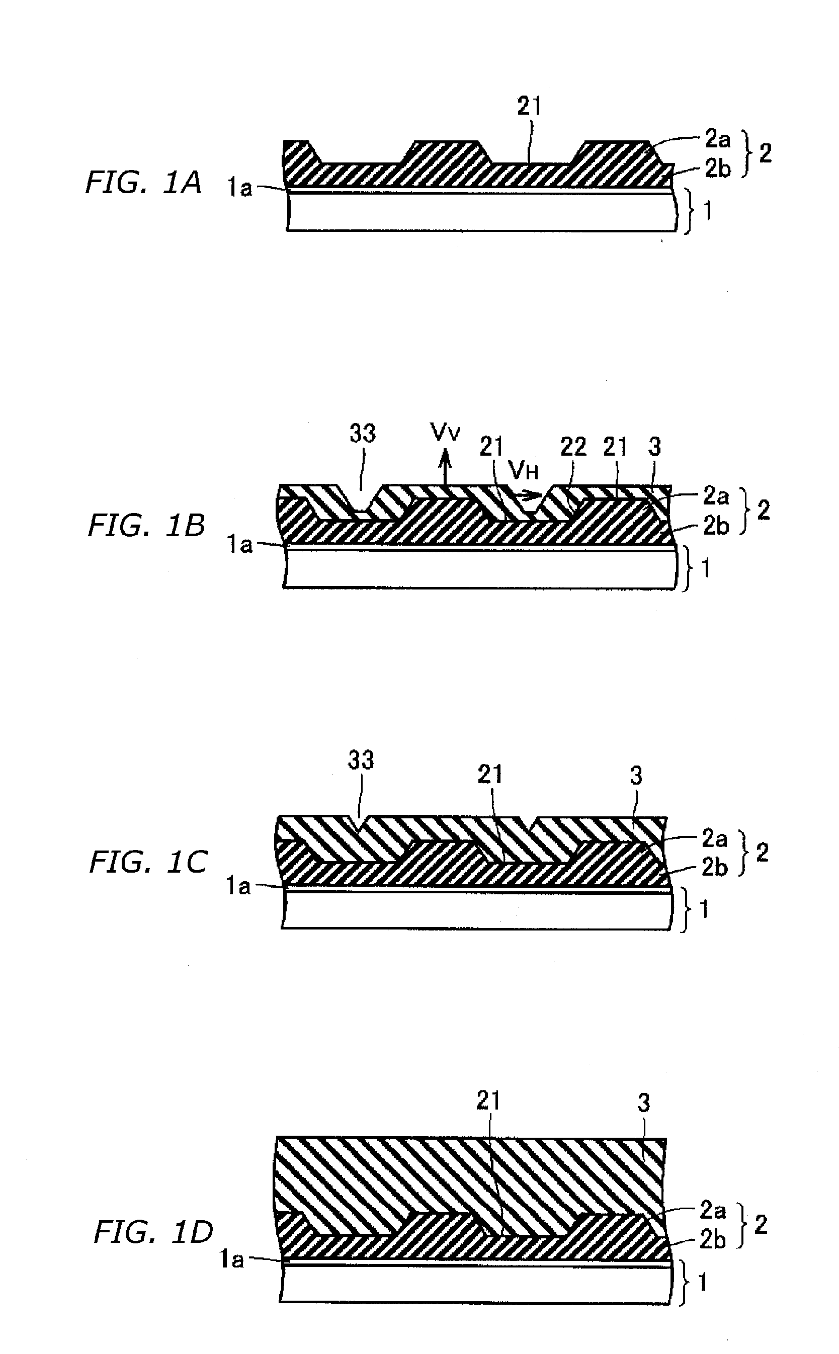
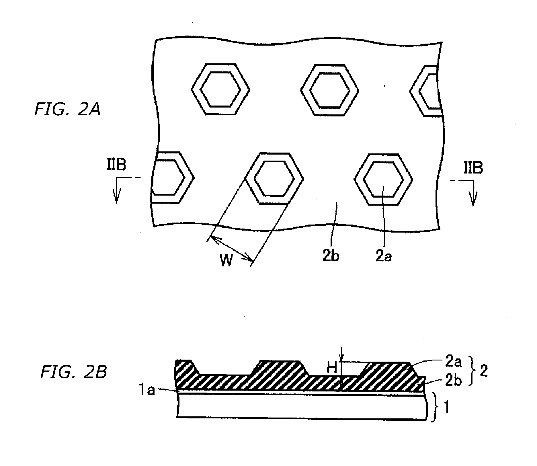
[0053] Reference is made to FIG. 1. GaN crystal as a first Group-III nitride crystal 2 was grown by a flux growth technique on the (0001) plane of a wurtzitic GaN substrate, serving as the base substrate 1, having a dislocation density of 1×10⁸ / cm2 and measuring 10 mm×10 mm×300 μm thickness, a 10 mm×10 mm face being the (0001) plane. Specifically, as illustrated in FIG. 5, the GaN substrate was arranged in the center of an alumina crucible, serving as a reaction chamber 4, with the (0001) plane facing upward, and 2.0 g metallic Ga and 1.0 g metallic Na (Na flux) were put into the alumina crucible and heated to form on the (0001) plane of the GaN substrate 800° C. molten Ga—Na, as a melt 7, (the surface level of the melt was 2 mm); and by supplying N2 gas into the Ga—Na melt for 3 hours to bring the pressure to 50 MPa, GaN crystal, having features 2a being in the form of hexagons when viewed from overhead and trapezoidal in section, as illustrated in FIG. 2, was produced as the first...

example 2

[0056] GaN crystal as a first Group-III nitride crystal was grown on a GaN substrate by a flux growth technique in the same manner as in Example 1. The dislocation density of the features of the first Group-III nitride crystal was 7×10⁵ / cm2, and the average dislocation density overall of the features and the floor was 8×10⁶ / cm2.

[0057] Next, GaN crystal as a second Group-III nitride crystal 3 was grown on the first Group-III nitride crystal by HVPE. Specifically, onto the substrate on which the first Group-III nitride crystal had been grown and in a molar ratio of 10:1000:7000, GaCl gas, NH3 gas, and H2 gas (carrier gas) were supplied at 1030° C. and 101 kPa and at a total gas flow rate of 8010 sccm for 1 hour to grow a 5 μm-thick GaN crystal as a second Group-III nitride crystal, whereby a GaN crystal substrate was produced. In this case, the dislocation density of the second Group-III nitride crystal was 7×10⁶ / cm2. The surface roughness Rp-v was 0.5 μm, and hexagonally shaped feat...


PUM

PropertyMeasurementUnit
roughnessaaaaaaaaaa
peak-to-valley roughnessaaaaaaaaaa
heightaaaaaaaaaa

Abstract

Affords a Group-III nitride crystal substrate that is of low dislocation density and is inexpensive to manufacture, a method of manufacturing such a substrate, and Group-III nitride semiconductor devices that incorporate the Group-III nitride crystal substrate. The Group-III nitride crystal substrate manufacturing method includes: a step of growing, by liquid-phase epitaxy, a first Group-III nitride crystal (2) onto a base substrate (1); and a step of growing, by vapor-phase epitaxy, a second Group-III nitride crystal (3) onto the first Group-III nitride crystal (2). The Group-III nitride crystal substrate, produced by such a manufacturing method, has a dislocation density of 1×10⁷ dislocations/cm2.

Description

BACKGROUND OF THE INVENTION [0001] 1. Field of the Invention [0002] The present invention relates to a Group-III nitride crystal substrate that is of low dislocation density and is inexpensive to manufacture, to a method of manufacturing such a substrate, and to Group-III nitride semiconductor devices that incorporate the Group-III nitride crystal substrate. [0003] 2. Description of the Background Art [0004] To serve as the substrates for semiconductor electronic and optoelectronic devices including semiconductor lasers and LEDs (light-emitting diodes), Group-III nitride crystal substrates of large size and low dislocation density are being pursued in recent years. [0005] To manufacture Group-III nitride crystal substrates, vapor-phase techniques enable crystal-growth rates of 100 μm / hr or greater; and among vapor-phase techniques, hydride vapor-phase epitaxy (HVPE hereinafter) is being utilized as powerful tool for rapid crystal growth. (Cf., for example, Isamu Akasaki, Group-III N...

Claims


Application Information

Patent Timeline
Patent Type & Authority Applications(United States)
IPC IPC(8): C30B19/02C30B25/18C30B29/40H01L21/205H01L21/20H01L21/208
CPCC30B7/10C30B9/10C30B19/02C30B25/18C30B29/406H01L21/02389H01L21/02625H01L21/02458H01L21/02494H01L21/0254H01L21/02587H01L21/0262H01L21/02433H01Q13/08
Inventor HIROTA, RYUNAKAHATA, SEIJIUENO, MASAKI
Owner SUMITOMO ELECTRIC IND LTD
Why Eureka
Try Eureka