Silicon Carbide on Diamond Substrates and Related Devices and Methods

a silicon carbide and diamond technology, applied in semiconductor devices, semiconductor/solid-state device details, electrical apparatus, etc., can solve the problems of reducing device performance, excessive heat can raise several problems, and the material of simiconductor materials cannot penetrate higher-power high-frequency applications to the extent desirable, so as to reduce the junction temperature and improve reliability, the effect of increasing the power density during operation

Active Publication Date: 2005-07-28
WOLFSPEED INC
View PDF45 Cites 76 Cited by
  • Summary
  • Abstract
  • Description
  • Claims
  • Application Information

AI Technical Summary

Benefits of technology

[0015] In one aspect, the invention is a method of forming a high-power, high-frequency device in wide bandgap semiconductor materials with reduced junction temperature, higher power density during operation or improved reliability at a rated power density or any combination of these advantages. In this aspect, the invention comprises adding a layer of diamond to a silicon carbide wafer to increase the thermal conductivity of the resulting composite wafer, thereafter reducing the thickness of the silicon carbide portion of the composite wafer while retaining sufficient thickness of silicon carbide to support epitaxial growth thereon, preparing the silicon carbide surface of the composite wafer for epitaxial growth thereon, and adding a Group IIII nitride heterostructure to the prepared silicon carbide face of the wafer.
[0016] In another aspect, the invention is a high-power, wide-bandgap device that exhibits reduced junction temperature and higher power density during operation and improved reliability at a rated power density. In this aspect, the invention comprises a diamond substrate for providing a heat sink with a thermal conductivity greater than silicon carbide, a single crystal silicon carbide layer on the diamond substrate for providing a supporting crystal lattice match for wide-bandgap material structures that is better than the crystal lattice match of diamond, and a Group IIII nitride heterostructure on the single crystal silicon carbide layer for providing device characteristics.

Problems solved by technology

These semiconductor materials have failed to penetrate higher power high frequency applications to the extent desirable, however, because of their relatively small bandgaps (e.g., 1.12 eV for Si and 1.42 for GaAs at room temperature) and relatively small breakdown voltages.
Excessive heat can raise several problems.
Higher temperatures also permit more tunneling and leaking that reduce device performance, and accelerate degradation and device failure.
Sapphire is relatively inexpensive and widely available, but is a poor thermal conductor and therefore unsuitable for high-power operation.
Additionally, in some devices, conductive substrates are preferred and sapphire lacks the capability of being conductively doped.
Silicon carbide has a better thermal conductivity than sapphire, a better lattice match with Group IIII nitrides (and thus encourages higher quality epilayers), and can be conductively doped, but is also much more expensive.
Furthermore, although progress has been made in designing and demonstrating GaN / AlGaN HEMTs on silicon carbide (e.g., the patents and published applications cited above) a lack of consistent reliability at desired rated performance parameters continues to limit commercial development.

Method used


Image

  • Silicon Carbide on Diamond Substrates and Related Devices and Methods
  • Silicon Carbide on Diamond Substrates and Related Devices and Methods
  • Silicon Carbide on Diamond Substrates and Related Devices and Methods

Examples


Embodiment Construction

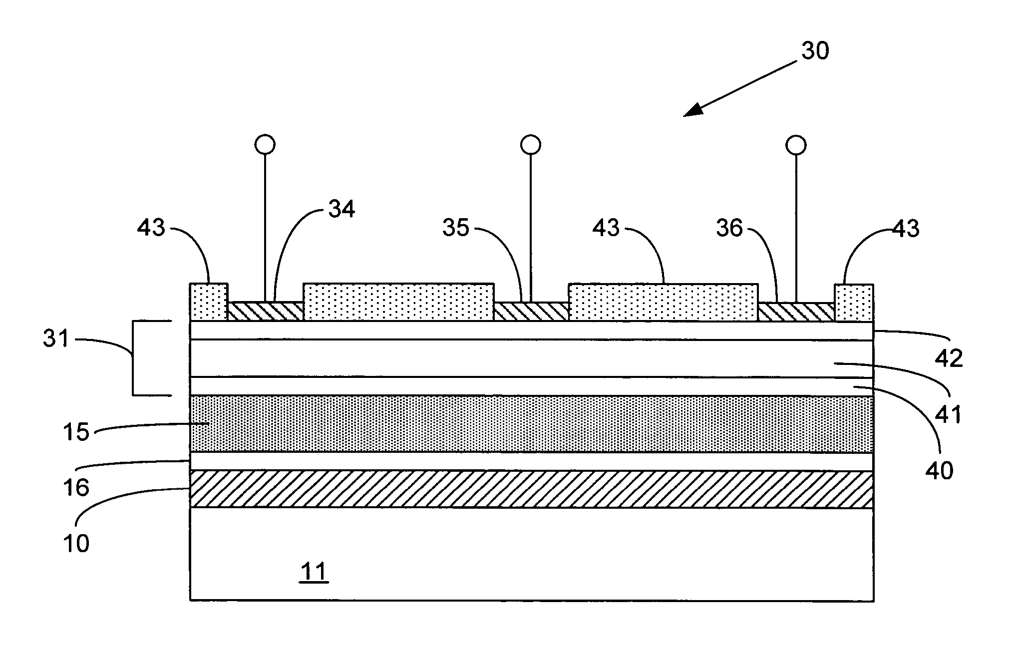
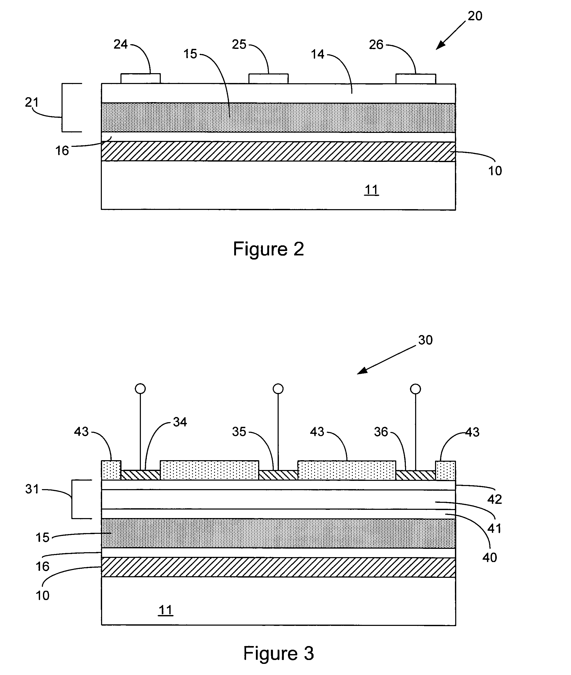
[0026] It will be understood that the advantages of the invention as described herein are neither exclusive of one another nor are they necessarily cumulative. Thus, by reducing the junction temperature, higher power density can be achieved at a given rated reliability, or the reliability can be increased at a previously-available rated power density, or some combination of these (and other) advantages can be achieved.

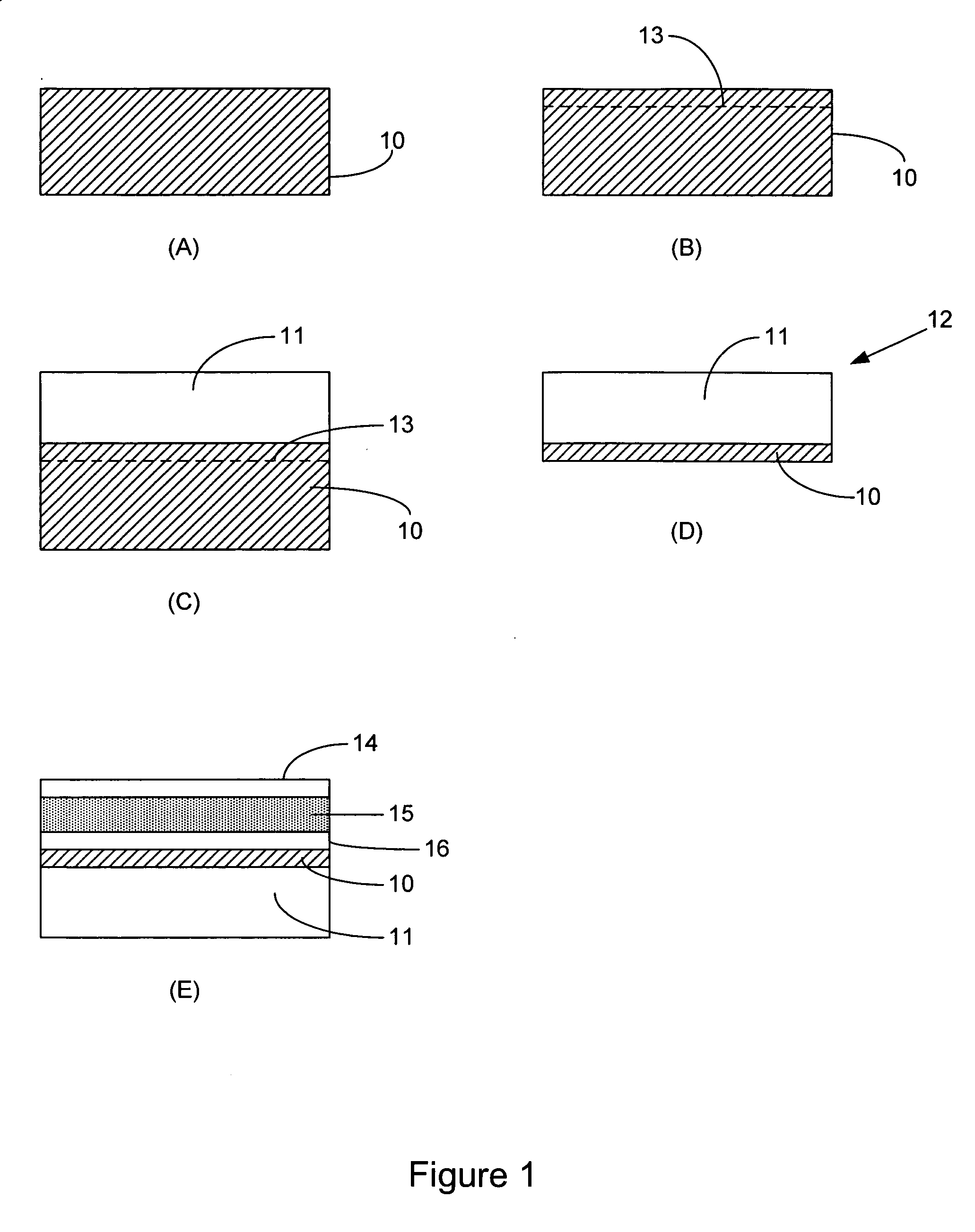
[0027] In a first embodiment, the invention is a method of forming a high-powered device in wide bandgap materials with reduced junction temperature, higher power density during operation, and improved reliability at a rated power density. The method is illustrated schematically in FIG. 1 which includes sub-Figures (A) through (E). FIG. 1 illustrates a silicon carbide wafer 10. In preferred embodiments and as is most useful for device structures, the silicon carbide wafer or substrate 10 is a single crystal layer that provides a highly suitable substrate for the Group...


PUM

PropertyMeasurementUnit
thickaaaaaaaaaa
thickaaaaaaaaaa
diameteraaaaaaaaaa

Abstract

A method of forming a high-power, high-frequency device in wide bandgap semiconductor materials with reduced junction temperature, higher power density during operation and improved reliability at a rated power density is disclosed, along with resulting semiconductor structures and devices. The method includes adding a layer of diamond to a silicon carbide wafer to increase the thermal conductivity of the resulting composite wafer, thereafter reducing the thickness of the silicon carbide portion of the composite wafer while retaining sufficient thickness of silicon carbide to support epitaxial growth thereon, preparing the silicon carbide surface of the composite wafer for epitaxial growth thereon, and adding a Group III nitride heterostructure to the prepared silicon carbide face of the wafer.

Description

BACKGROUND OF INVENTION [0001] The present invention relates to semiconductor devices formed of materials that make them suitable for high power, high temperature, and high frequency applications. As known to those familiar with semiconductors, materials such as silicon (Si) and gallium arsenide (GaAs) have found wide application in semiconductor devices for lower power and (in the case of Si) lower frequency applications. These semiconductor materials have failed to penetrate higher power high frequency applications to the extent desirable, however, because of their relatively small bandgaps (e.g., 1.12 eV for Si and 1.42 for GaAs at room temperature) and relatively small breakdown voltages. [0002] Accordingly, interest in high power high temperature and high frequency applications and devices has turned to wide bandgap semiconductor materials such as silicon carbide (2.996 eV for alpha SiC at room temperature) and the Group III nitrides (e.g., 3.36 eV for gallium nitride at room t...

Claims


Application Information

Patent Timeline
Patent Type & Authority Applications(United States)
IPC IPC(8): H01L21/20H01L23/373H01L29/778
CPCH01L21/02378H01L21/02527H01L29/778H01L29/1602H01L21/0254H01L21/20
Inventor SAXLER, ADAM WILLIAM
Owner WOLFSPEED INC
Why Eureka
Try Eureka