Semiconductor radiation detector, positron emission tomography apparatus, semiconductor radiation detection apparatus, detector unit and nuclear medicine diagnostic apparatus

a semiconductor radiation and detector technology, applied in the direction of optical radiation measurement, instruments, x/gamma/cosmic radiation measurement, etc., can solve the problems of reducing the probability of holes being annihilated midway the distance, shortening the distance up to the electrodes, etc., to facilitate maintenance and examination, shorten the time required to mount the semiconductor radiation detectors on the nuclear medicine diagnostic apparatus, the effect of shortening the tim

Inactive Publication Date: 2005-08-04
AMEMIYA KENSUKE +7
View PDF5 Cites 4 Cited by
  • Summary
  • Abstract
  • Description
  • Claims
  • Application Information

AI Technical Summary

Benefits of technology

[0011] In order to solve the above described problems, a first embodiment of the present invention improves detection sensitivity by shortening a distance between electrodes for charge collection of a semiconductor radiation detector. That is, the distance between an anode electrode and cathode electrode or the thickness of a semiconductor area sandwiched between the anode electrode and cathode electrode is 0.2 to 2 mm. In this structure, the distance from positions of electrons and holes generated by interaction between the semiconductor material and radiation to the electrodes is shortened, and therefore the time required for them to reach the electrodes is shortened. Furthermore, shortening the distance up to the electrodes reduces the probability that holes may be annihilated midway the distance.
[0012] A second embodiment of the present invention is a nuclear medicine diagnostic apparatus comprising a plurality of unit substrates including a plurality of semiconductor radiation detectors for introducing radiation and an integrated circuit for processing radiation detection signals output from the plurality of semiconductor radiation detectors. This allows the semiconductor radiation detectors and the integrated circuits which process the outputs to be disposed close to one another, with the result that when weak output signals of the semiconductor radiation detectors are transmitted to the integrated circuits, it is possible to reduce influences of noise on the weak output signals.
[0013] The semiconductor radiation detector, analog LSI (Large Scale Integrated Circuit), AD converter and digital LSI are preferably arranged on the unit substrate in that order and the respective elements are connected by wiring so that a signal detected by the semiconductor radiation detector is processed by the analog LSI, the signal processed by the analog LSI is processed by the AD converter, and the signal processed by the AD converter is processed by the digital LSI. By shortening the distance between the semiconductor radiation detector and analog LSI in particular, this structure can shorten the wiring distance between the semiconductor radiation detector and analog LSI and thereby reduce noise superimposed on the wiring until the signal detected by the semiconductor radiation detector reaches the analog LSI. In an embodiment which will be described later, the LSI (integrated circuit) corresponds to an ASIC. Also, the semiconductor radiation detection apparatus corresponds to a combined substrate (detector substrate+ASIC substrate) in the embodiment which will be described later.

Problems solved by technology

Furthermore, shortening the distance up to the electrodes reduces the probability that holes may be annihilated midway the distance.

Method used


Image

  • Semiconductor radiation detector, positron emission tomography apparatus, semiconductor radiation detection apparatus, detector unit and nuclear medicine diagnostic apparatus
  • Semiconductor radiation detector, positron emission tomography apparatus, semiconductor radiation detection apparatus, detector unit and nuclear medicine diagnostic apparatus
  • Semiconductor radiation detector, positron emission tomography apparatus, semiconductor radiation detection apparatus, detector unit and nuclear medicine diagnostic apparatus

Examples


embodiment 1

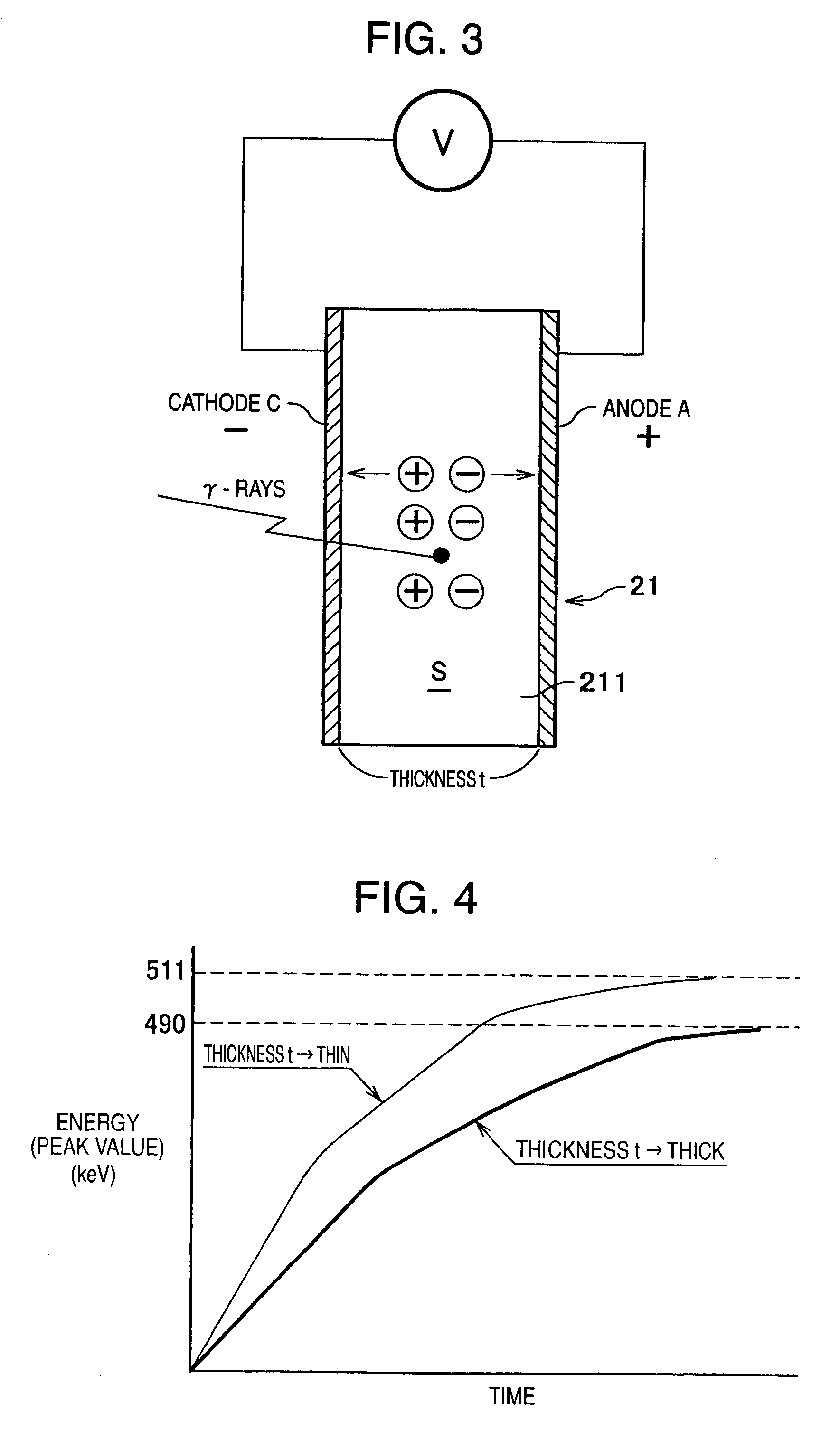
[0036] A nuclear medicine diagnostic apparatus which is a preferred embodiment of the present invention will be explained with reference to attached drawings in detail below as appropriate. The following are explanations of the nuclear medicine diagnostic apparatus according to this embodiment, distance between electrodes of a semiconductor radiation detector, arrangement (layout) of elements such as analog ASIC on a substrate, and elements applicable to this embodiment for construction of substrate units, etc. Note that an analog ASIC refers to an ASIC (Application Specific Integrated Circuit) which is an application-specific IC for processing analog signals and is a kind of LSI.

Nuclear Medicine Diagnostic Apparatus

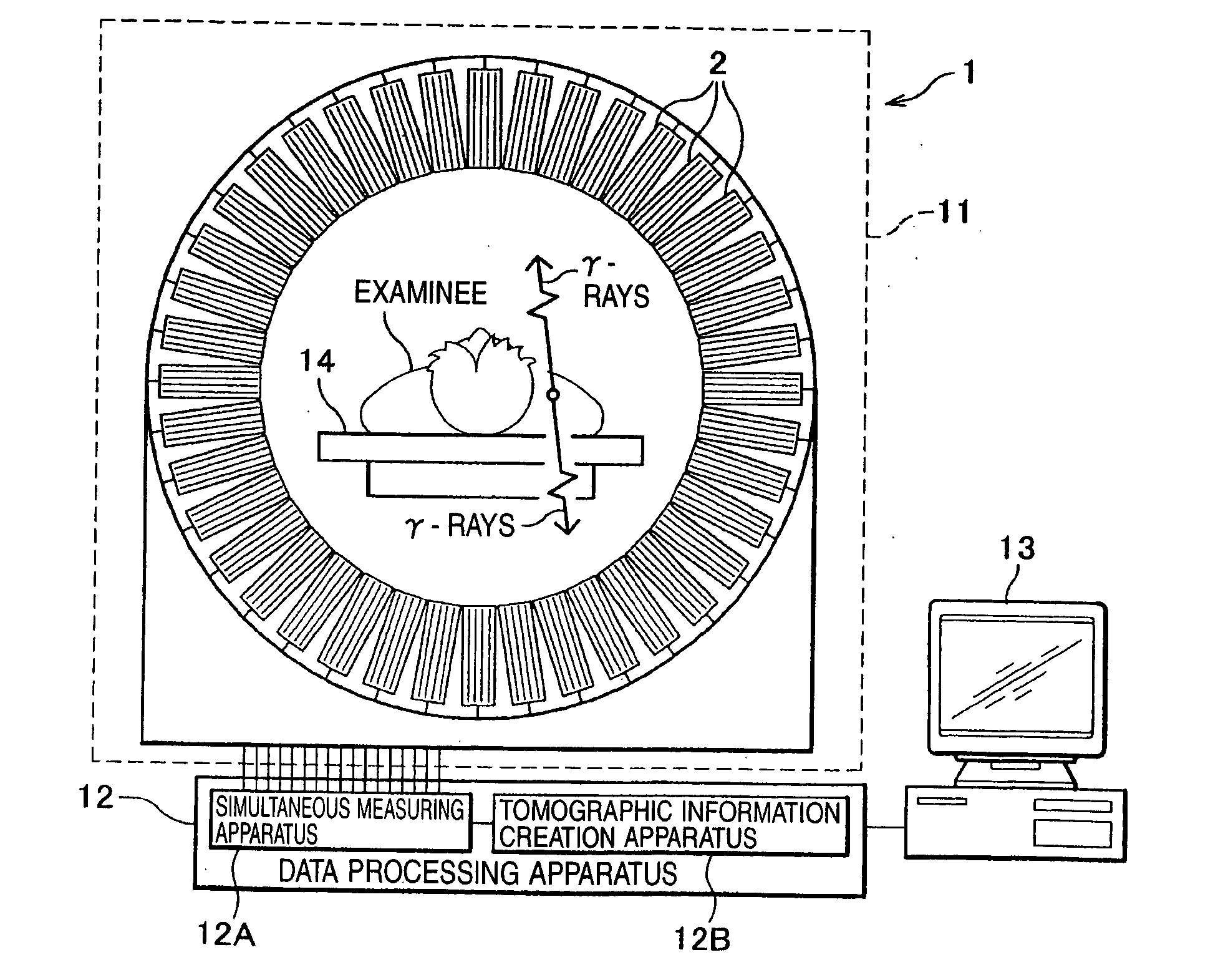
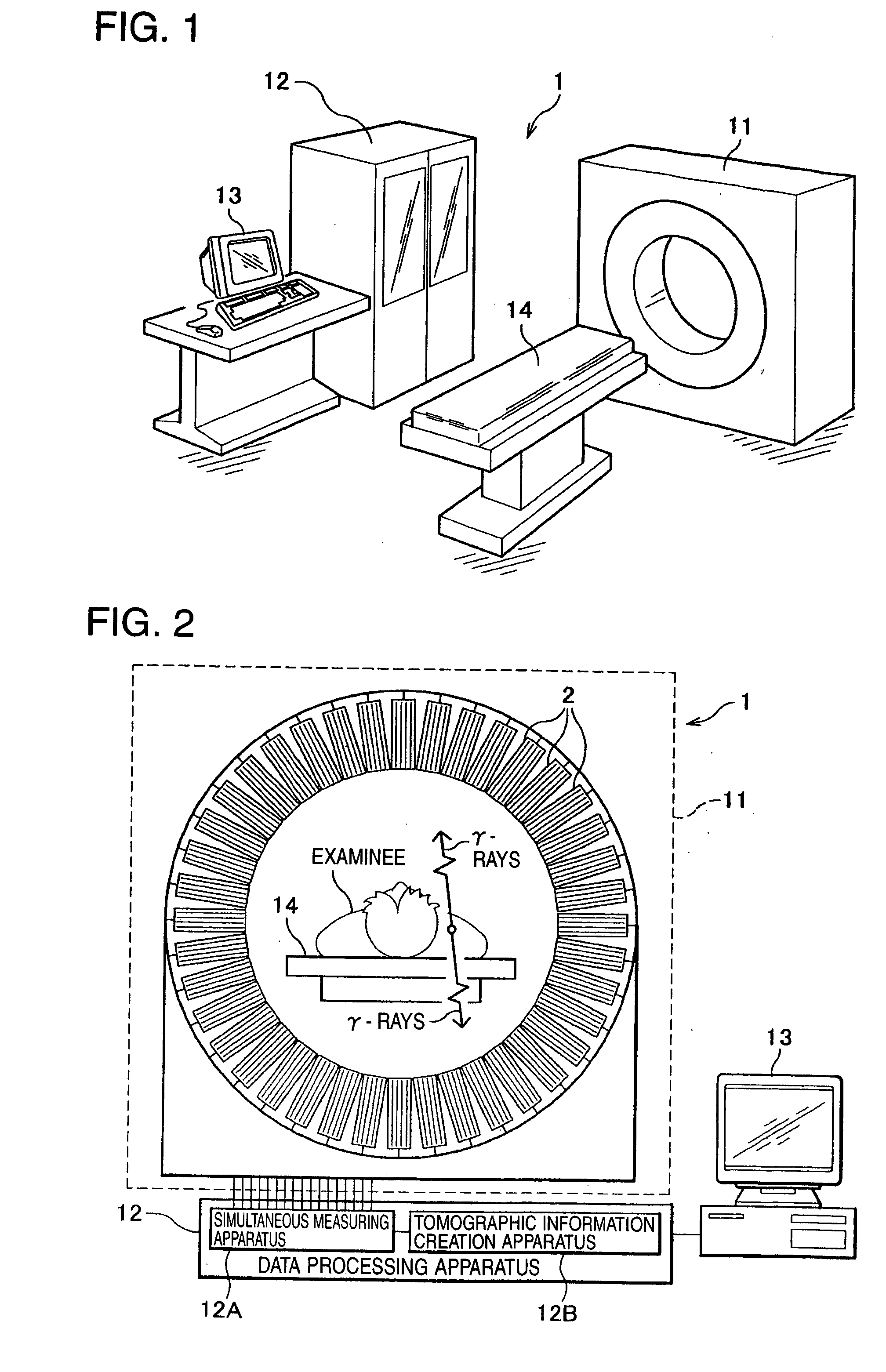
[0037] First, the nuclear medicine diagnostic apparatus (radiological diagnostic apparatus) according to this embodiment will be explained. As shown in FIG. 1, a PET apparatus 1 as the nuclear medicine diagnostic apparatus is constructed by including a camera (image p...

embodiment 2

[0101] A nuclear medicine diagnostic apparatus according to another embodiment will be explained. The nuclear medicine diagnostic apparatus of this embodiment is single photon emission computer tomography (SPECT) apparatus.

[0102] This SPECT apparatus 51 will be explained using FIGS. 13 to 15. The SPECT apparatus 51 is provided with a pair of radiation detection blocks 52, a rotary holder (body of rotation) 57, a data processing apparatus 12A and a display apparatus 13. The radiation detection blocks 52 are disposed at two positions with a 180° difference in the circumferential direction of the rotary holder 57. More specifically, the respective unit support members 56 of the radiation detection blocks 52 are mounted on the rotary holder 57 with a 180° difference in the circumferential direction. A plurality of detector units 2A each including twelve combined substrates 53 are mounted on the respective unit support members 56 in a detachable / attachable manner. Thus, the detectors 21...


PUM


Abstract

Each semiconductor radiation detector used for a nuclear medicine diagnostic apparatus (PET apparatus) is constructed with an anode electrode A facing a cathode electrode C sandwiching a CdTe semiconductor member S which generates charge through interaction with γ-rays. Then, a thickness t of the semiconductor member S sandwiched between these mutually facing anode electrode A and cathode electrode C is set to 0.2 to 2 mm. Furthermore, the devices are mounted (laid out) on substrates in such a way that the distance (distance of conductor) between the semiconductor radiation detector and an analog ASIC which processes the signal detected by this detector is shortened. Furthermore, the substrates on which the detectors are mounted are housed in a housing as a unit (detector unit).

Description

CROSS-REFERENCE TO RELATED APPLICATION [0001] The present application is related to a U.S. Ser. No. ______ being filed based on Japanese Patent Application No. 2003-342437 filed on Sep. 30, 2003, the entire content of which is incorporated herein by reference. BACKGROUND OF THE INVENTION [0002] The present invention relates to a nuclear medicine diagnostic apparatus, and more particularly, to a positron emission tomography (hereinafter referred to as “PET”) apparatus, which is a kind of a nuclear medicine diagnostic apparatus using a semiconductor radiation detector, semiconductor radiation detection apparatus or detector unit. [0003] A detector using a NaI scintillator is known as a conventional radiation detector for detecting radiation such as γ-rays. With a gamma camera (a kind of nuclear medicine diagnostic apparatus) provided with a NaI scintillator, radiation (γ-rays) incident on the scintillator at an angle restricted by many collimators interacts with NaI crystals and emits...

Claims


Application Information

Patent Timeline
Patent Type & Authority Applications(United States)
IPC IPC(8): G01T1/24G01J1/00G01T1/161G01T1/164G01T1/166G01T1/29H01L27/14H01L31/09
CPCG01T1/2985G01T1/2928
Inventor AMEMIYA, KENSUKEUENO, YUUICHIROUKITAGUCHI, HIROSHIYOKOMIZO, OSAMUKOJIMA, SHINICHITSUCHIYA, KATSUTOSHIYANAGITA, NORIHITOYOKOI, KAZUMA
Owner AMEMIYA KENSUKE
Why Eureka
Try Eureka