Method for fabrication of semiconductor device

a semiconductor device and fabrication method technology, applied in semiconductor devices, semiconductor/solid-state device details, electrical equipment, etc., can solve the problems of increasing the cost of mask sets required for each new process technology, increasing the cost of product development, and reducing manufacturing flexibility. , to achieve the effect of saving mask costs, saving silicon, and increasing flexibility

Inactive Publication Date: 2005-08-04
INTEL CORP
View PDF28 Cites 3 Cited by
  • Summary
  • Abstract
  • Description
  • Claims
  • Application Information

AI Technical Summary

Benefits of technology

[0015] The prior art reflected the motivation to better fit the device size to the custom application and therefore saving on wasted silicon. The current invention reflects the motivation to save the cost of mask with respect to the investment that would have been otherwise required to put in place proper set of master slices. The current invention also seeks to provide the ability to incorporate memory block in the custom device. The current invention provides a method to customize the device with respect the amount of logic and memory required.
[0016] The main point of the current invention is the use of area I/O to provide a continuous fabric that provides a continuous terrain of logic and I/O and also provides the ability to mix in continuous terrain of memory with islands of special functions like PLL and SERDES. The current invention shows that with area I/O and redistribution layer to connect the area I/O to area pads, many of the limitation of the prior art are overcome. A greater level of flexibility is therefore provided. The current invention also suggests to utilize Module Array, whereby additional layers such as Metal-1 and Metal-2 are generic and would be part of such borderless continuous terrain. Furthermore, the current invention also suggests the use of segmented routing whereby some of the connectivity layers are also generic and would be a part of the continuous terrain. In such fabric only few layers need to be customized while most of the layers are generic and consist primarily of a repeating pattern. A favorable embodiment of the current invention is a continuous terrain customizable by single custom via layer. Furthermore, the current invention suggests the use of direct-write e-Beam for those few custom layers. An added advantage of the current invention is the use of direct-write e-Beam on the continuous terrain to provide on the same wafer different product types, with different amount of product units of the various product types. The very large size of current wafer allows hundreds of device units, each of different type, built on a single wafer. Therefore the current invention allows to provide “on-demand” semiconductor device manufacturing, where one customers could get few units of one type of device for prototype work, while an

Problems solved by technology

Semiconductor manufacturing is known to improve device density in exponential manner over time, but such improvements do come with a price.
The cost of mask set required for each new process technology has been increasing exponentially.
These changes represent an increasing challenge primarily to custom products, which tend to target smaller volume and less diverse market, therefore making the increased cost of product development and reduction of manufacturing flexibility ver

Method used


Image

  • Method for fabrication of semiconductor device
  • Method for fabrication of semiconductor device
  • Method for fabrication of semiconductor device

Examples


Embodiment Construction

[0100] The present invention is now described with reference to FIGS. 1-25, it being appreciated that the figures illustrate the subjects matter not to scale or to measure.

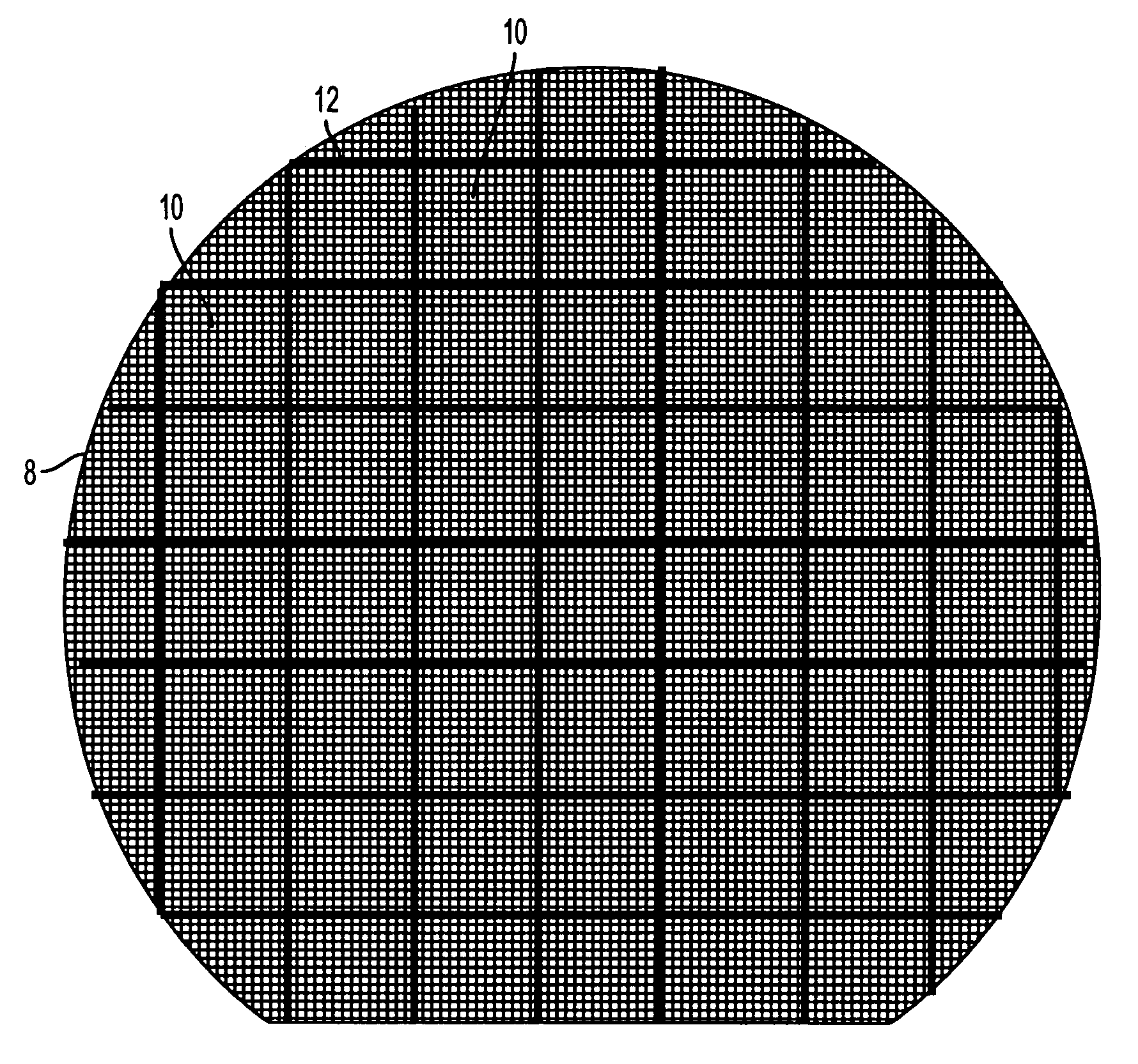
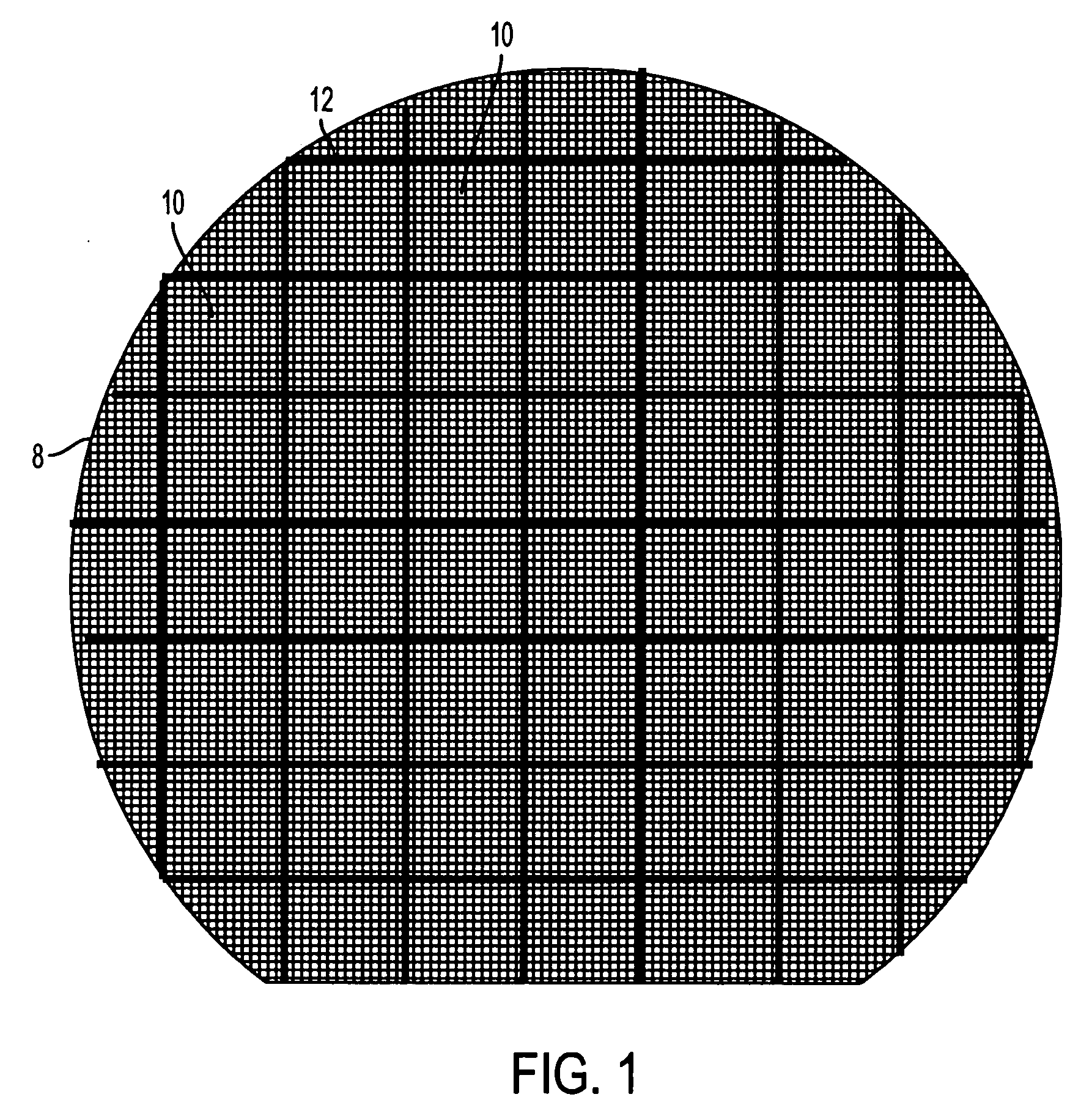
[0101] The current method of semiconductor fabrication is on lithography step for each layer. The dominating lithography technique of submicron process is called step and repeat. The layer pattern will be drawn into mask also called reticle. Such reticle may be projected over an area of about 20 mm×20 mm by the lithography tool called Stepper. Then the Stepper steps the wafer so the reticle would be projecting the same pattern on area next to it and so for. FIG. 1 illustrates a wafer 8 with marks 12 of reticle projections 10. With an 8-inch wafer, over 50 copies of the reticle will be typically stepped on one such wafer.

[0102] The current invention suggests the use of a much less common lithography technique called direct-write using e-Beam. Such could be done, for example, with direct-write e-Beam—Leica ZBA32 o...


PUM


Abstract

A novel method is presented to provide ASICs with drastically reduced NRE and with volume flexibility. The invention includes a method of fabricating an integrated circuit, including the steps of: providing a semiconductor substrate, forming a borderless logic array including a plurality of Area I/Os and also including the step of forming redistribution layer for redistribution at least some of the Area I/Os for the purpose of the device packaging. The fabrication may utilize Direct Write e-Beam for customization. The customization step may include fabricating various types of devices at different volume from the same wafer.

Description

BACKGROUND OF THE INVENTION [0001] 1. Field of the Invention [0002] The present invention relates to logic arrays and fabrication method for custom integrated circuit [0003] 2. Discussion of Background Art [0004] Semiconductor manufacturing is known to improve device density in exponential manner over time, but such improvements do come with a price. The cost of mask set required for each new process technology has been increasing exponentially. In addition, the minimum fabrication quantity due to the increases of wafer size has also increased exponentially at the same time. [0005] These changes represent an increasing challenge primarily to custom products, which tend to target smaller volume and less diverse market, therefore making the increased cost of product development and reduction of manufacturing flexibility very hard to accommodate. [0006] Custom Integrated Circuits can be segmented into two groups. The first are devices that have all their layers custom made. The second ...

Claims


Application Information

Patent Timeline
IPC IPC(8): H01L21/44H01L23/34H01L23/48H01L23/525H01L27/10
CPCH01L23/525H01L2924/14H01L2924/3011H01L2924/0002H01L2924/00
Inventor OR-BACH, ZVICOOKE, LAURANCE
Owner INTEL CORP
Why Eureka
Try Eureka