Single-poly 2-transistor based fuse element

a fuse element and single-poly-transistor technology, applied in the field of integrated circuits, can solve the problems of reliability concerns, damage to the device passivation layer, and hole in the passivation layer, and achieve the effect of reducing the programming voltage of the fuse and increasing the capacitive coupling

Inactive Publication Date: 2005-08-04
INFINEON TECH AG
View PDF28 Cites 19 Cited by
  • Summary
  • Abstract
  • Description
  • Claims
  • Application Information

AI Technical Summary

Benefits of technology

[0009] The present invention achieves technical advantages as an electrically programmable transistor fuse having a source and drain disposed in a semiconductor substrate and further having a double-gate arrangement disposed in a single layer of polysilicon in which one gate is capacitively couple to the drain region. The transistor fuse further includes a coupling device adapted to increase the capacitive coupling of the one gate and the drain region for enabling reduction in fuse programming voltage, wherein programming of the transistor fuse is effectuated via application of a voltage signal to the drain in which the voltage signal is less than the junction breakdown of the transistor fuse.

Problems solved by technology

This and other similar approaches can result in damage to the device passivation layer, and thus, lead to reliability concerns.
For example, the process of programming the fuse can cause a hole in the passivation layer when the fuse material is displaced.
Also the method is not in-system, sometimes inconvenient, and thus lead to higher test cost.
Since significant energy or high programming current is required to pass through these devices to reach the passive element, the size required for the programming (pass gate) transistors can be very large.
The programming process results in a damaged gate-oxide which reduces the electrical resistance across the oxide.
Because of the significant energy required for programming, damage can result to surrounding structure and / or unreliable sensing can result because of the inconsistent nature of the blow process and the relatively small change typically offered in the programmed resistance.
Further, these type of devices may not be viable for use with many of the latest process technologies because of the required programming potentials, i.e. high current flow and high voltage levels over a requisite amount of time.

Method used


Image

  • Single-poly 2-transistor based fuse element
  • Single-poly 2-transistor based fuse element
  • Single-poly 2-transistor based fuse element

Examples


Embodiment Construction

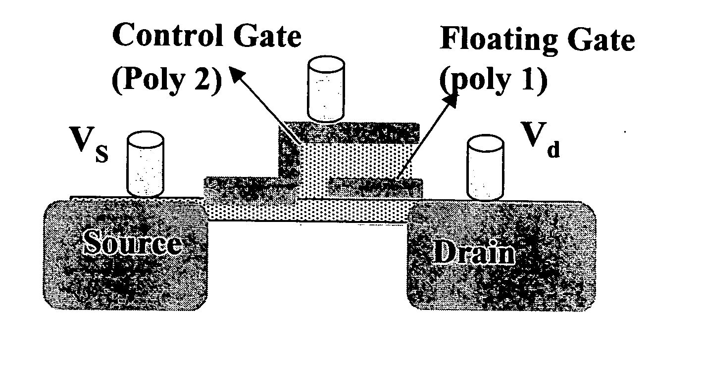
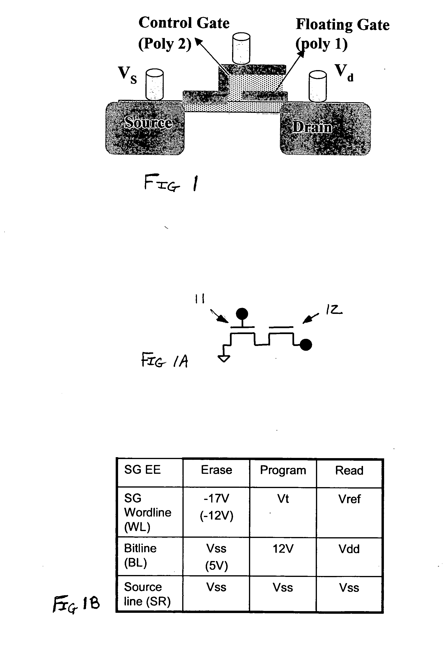
[0024] The numerous innovative teachings of the present application will be described with particular reference to the presently preferred exemplary embodiments. However, it should be understood that this class of embodiments provides only a few examples of the many advantageous uses and innovative teachings herein. In general, statements made in the specification of the present application do not necessarily delimit any of the various claimed inventions. Moreover, some statements may apply to some inventive features, but not to others. Throughout the drawings, it is noted that the same reference numerals or letters will be used to designate like or equivalent elements having the same function. Detailed Descriptions of known functions and constructions unnecessarily obscuring the subject matter of the present invention have been omitted for clarity.

[0025] Current electrical fuses are passive elements, such as resistors or capacitors, which are programmed by electrical pulses with t...


PUM


Abstract

An electrically programmable transistor fuse having a double-gate arrangement disposed in a single layer of polysilicon in which a first gate is disposed overlapping a portion of a source region and a second gate is insulated from the first gate and disposed overlapping a portion of a drain region. The first gate includes a terminal for receiving an externally applied control signal and the second gate is capacitively couple to the drain region in which a coupling device is included for increasing the capacitive coupling of the second gate and the drain region for enabling reduction in fuse programming voltage.

Description

BACKGROUND OF THE INVENTION [0001] 1. Technical Field of the Invention [0002] The invention relates generally to the field of integrated circuit and, more particularly, to fusible link programming in semiconductor integrated circuits. [0003] 2. Description of Related Art [0004] In integrated circuits including CMOS integrated circuits, it is often desirable to be able to permanently store information, or to form permanent connections of the integrated circuit after it is manufactured. Fuse or anti-fuse devices forming fusible links are frequently used for this purpose. Fuses and anti-fuses can also be used to program redundant elements to replace identical defective elements such as DRAM, Flash EEPROM, SRAM, or other memories. Further, fuses can be used to store die identification or other such information, or to adjust the speed of a circuit by adjusting the resistance of the current path. [0005] One type of fuse device is “programmed” or “blown” using a laser to open a link after ...

Claims


Application Information

Patent Timeline
Patent Type & Authority Applications(United States)
IPC IPC(8): G11C16/04G11C29/00H01L21/336H01L23/525H01L27/115H01L29/788
CPCG11C16/0433G11C29/789G11C2216/10H01L23/5256H01L27/115H01L2924/0002H01L29/66825H01L29/7885H01L2924/00H10B69/00
Inventor KOTHANDARAMAN, CHANDRASEKHARANSHUM, DANNY
Owner INFINEON TECH AG
Why Eureka
Try Eureka