Plasma display panel and its manufacturing method

a technology of plasma display panel and manufacturing method, which is applied in the manufacture of electrode systems, discharge tube luminescnet screens, gas mixture absorption, etc., can solve the problems of prone to adsorption of large amount of h, difficult to add impurities, and difficult to diffuse impurity gas in discharge gas in a controlled manner, so as to and improve the effect of adsorption

Inactive Publication Date: 2005-08-04
PANASONIC CORP
View PDF6 Cites 0 Cited by
  • Summary
  • Abstract
  • Description
  • Claims
  • Application Information

AI Technical Summary

Benefits of technology

[0012] In order to attain this object, in the present invention, impurity gas other than inert gas is adsorbed by phosphor layers in a step of sealing the periphery of substrates or before the sealing step, so that the impurity gas is released into discharge gas while...

Problems solved by technology

However, it is extremely difficult to add impurity other than rare gas in a predetermined concentration to discharge gas uniformly in a controlled manner, in order to improve discharge characteristics.
Phosphor materials and magnesium oxide (MgO) serving as a protective film, which are structural materials of a PDP and in contact with discharge gas, are prone to adsorb a large amount of gas other than inert gas: thus, it is difficult to diffuse impurity gas in di...

Method used


Image

  • Plasma display panel and its manufacturing method
  • Plasma display panel and its manufacturing method
  • Plasma display panel and its manufacturing method

Examples


first exemplary embodiment

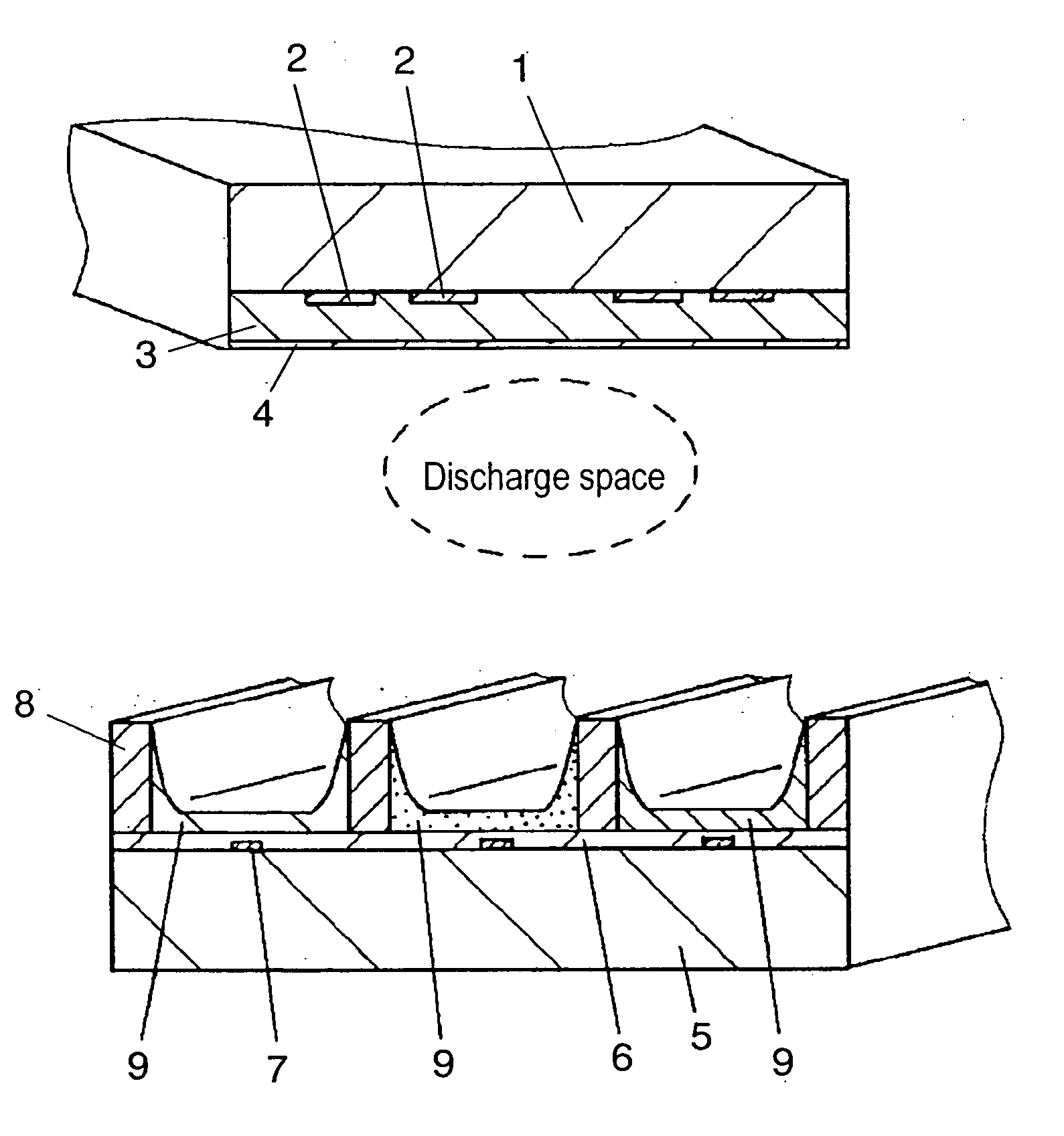
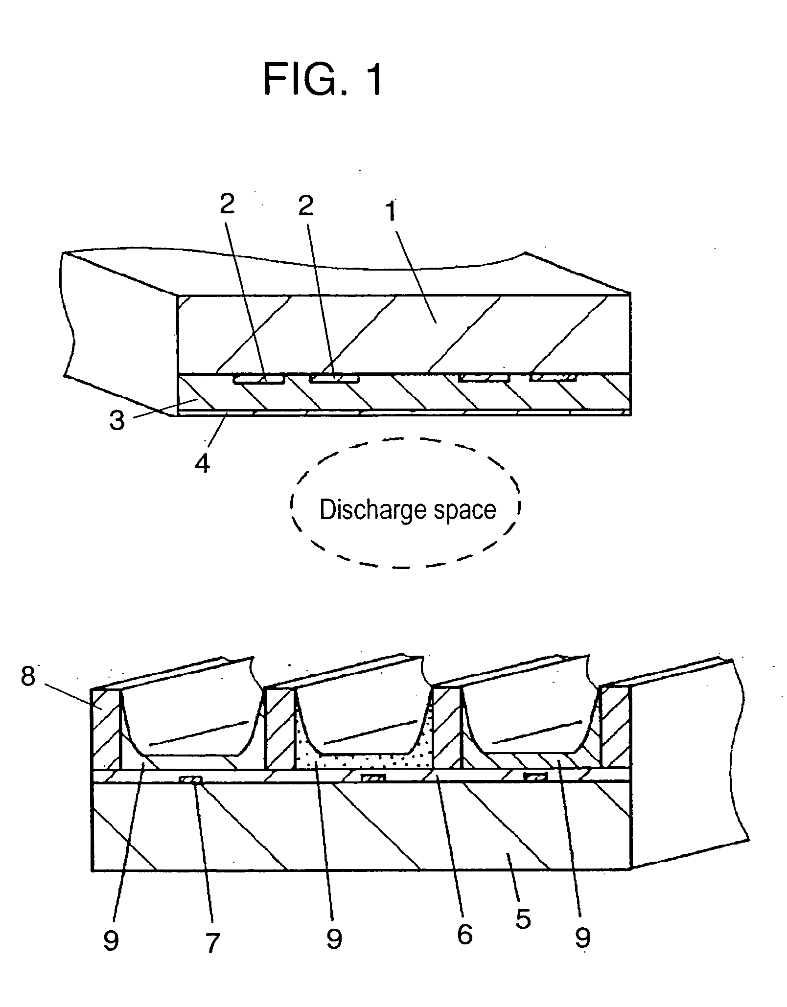
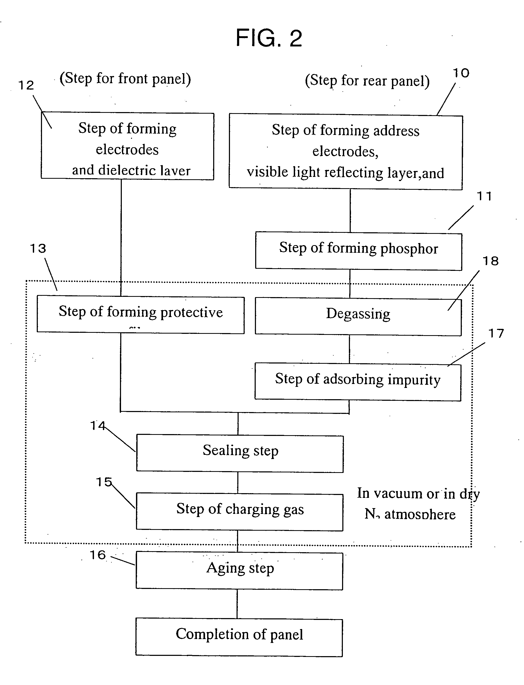
[0018] First, a description is provided of the first exemplary embodiment. FIG. 1 illustrates a structure of a PDP of the present invention. As shown in FIG. 1, a plurality of rows of stripe-like display electrodes 2, each made of a pair of a scan electrode and a sustain electrode, are formed on transparent substrate 1 made of material such as glass, on the front side. Dielectric layer 3 made of glass is formed so as to cover the electrodes. Formed on dielectric layer 3 is protective film 4 made of MgO.

[0019] On substrate 5 made of material such as glass, on the rear side, which is opposed to substrate 1 on the front side, a plurality of rows of stripe-like address electrodes 7 covered with visible light reflecting layer 6 made of dielectric glass are formed so as to intersect display electrodes 2, i.e. pairs of scan electrodes and sustain electrodes. On visible light reflecting layer 6 between these address electrodes 7, a plurality of ribs 8 are formed in parallel with address el...

second exemplary embodiment

[0058] Next, the second exemplary embodiment is described.

[0059] In the second exemplary embodiment, impurity gas containing at least CH4 is adsorbed by phosphor layers during or before the sealing step. Similar to the first exemplary embodiment, the impurity gas to be adsorbed is limited. For this purpose, glass substrates on front and rear sides are subjected to the steps surrounded by the dotted lines in FIG. 2 in a vacuum up to 10−4 Pa, or in a dry N2 atmosphere having a dew point up to −60° C. As for the glass substrate on the front side, all the steps from the formation of magnesium oxide, i.e. a protective film, by vacuum electron-beam evaporation to Step 15 of charging sealing gas are performed under the above conditions. As for the glass substrate on the rear side, all the steps after the firing phosphors to Step 15 are performed under the above conditions except for Step 17 of adsorbing impurity gas. The steps before and including the step of firing phosphors on the glass...


PUM


Abstract

A plasma display panel capable of realizing improvement in the characteristics thereof, such as lower discharge voltage, more stable discharge, higher luminance, higher efficiency, and longer life. During a step of sealing the periphery of substrates or before this sealing step, impurity gas other then inert gas is adsorbed by phosphor layers. The impurity gas is released into discharge gas and the impurity is added to the discharge gas in a controlled manner while the panel is lit. This method can realize improvement in characteristics, such as lower discharge voltage, higher luminance, higher efficiency, and longer life.

Description

FIELD OF THE INVENTION [0001] The present invention relates to a plasma display panel (hereinafter referred to as a “PDP”) employing gas discharge emission that is used as a color television receiver or a display for displaying characters or images. It also relates to a method of manufacturing the PDP. BACKGROUND OF THE INVENTION [0002] In a PDP, ultraviolet rays generated by gas discharge excite phosphors and cause them to emit light for color display. The PDP is structured so that display cells partitioned by ribs are provided on a substrate thereof, and a phosphor layer is formed on each of the display cells. [0003] The PDPs are roughly classified into an AC type and a DC type in terms of driving methods thereof. Discharge systems thereof include two types, i.e. a surface discharge type and an opposite discharge type. Having higher definition, a larger screen, and simpler manufacturing method, a surface discharge type having a three-electrode structure is mainly used in PDPs. Thi...

Claims


Application Information

Patent Timeline
IPC IPC(8): H01J9/02H01J9/24H01J11/42H01J9/38H01J9/39H01J11/50H01J17/20H01J17/24H01J17/26H01J17/49
CPCH01J9/261H01J9/38H01J11/52H01J11/12H01J11/42H01J9/395H01J9/02H01J9/24
Inventor NISHIMURA, MASAKIAKIYAMA, KOJIMIYASHITA, KANAKOAOTO, KOJIHORIKAWA, KEIJIYAMAUCHI, MASAAKI
Owner PANASONIC CORP
Why Eureka
Try Eureka