Signal line circuit device

a circuit device and signal line technology, applied in the direction of waveguides, high frequency circuit adaptations, addition of non-printed jumper connections, etc., can solve the problem of prone to fluctuations in the character of the signal line, and achieve the effect of adjusting the device characteristics

Active Publication Date: 2005-08-04
SANYO ELECTRIC CO LTD
View PDF5 Cites 20 Cited by
  • Summary
  • Abstract
  • Description
  • Claims
  • Application Information

AI Technical Summary

Benefits of technology

[0010] The present invention takes the circumstances described above into consideration, with an object of providing a technique that enables the signal line in a signal line circuit device to be trimmed easily, thus enabling adjustment of the device characteristics.

Problems solved by technology

If other members are positioned close to the signal line while the signal line is formed on the surface of the dielectric layer, then the characteristic impedance of the signal line is prone to fluctuations due to the effect of the neighboring members.

Method used


Image

  • Signal line circuit device
  • Signal line circuit device
  • Signal line circuit device

Examples


first embodiment

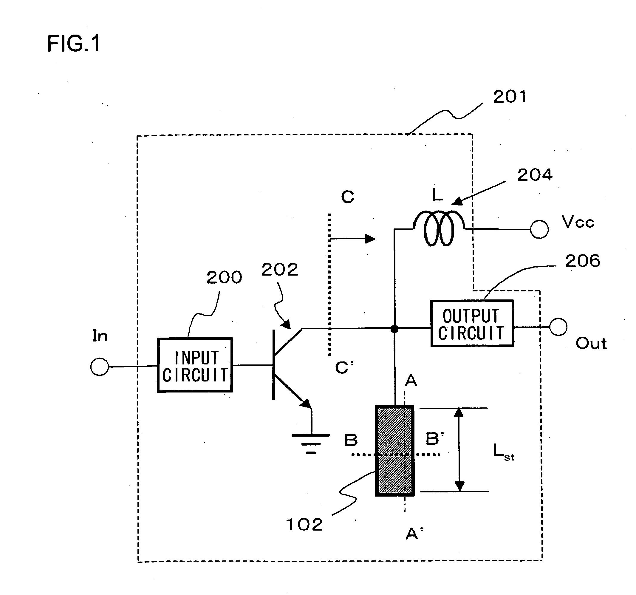
[0044]FIG. 1 is a diagram showing the layout of the peripheral circuits when a signal line circuit device according to a first embodiment of the present invention is used as one component of an amplifier.

[0045] In the diagram, the amplifier 201 comprises an input circuit 200, a transistor 202, a coil 204, a signal line circuit device 102, and an output circuit 206. The input circuit 200 is connected to the base of the transistor 202, and the output circuit 206 is connected to the collector. Furthermore, the coil 204 and the signal line circuit device 102 are also connected to the collector of the transistor 202. The emitter of the transistor 202 is grounded. A detailed description of the signal line circuit device 102 is presented below, but in brief, the signal line circuit device 102 is a microstrip line comprising a signal line and a ground line. The characteristics of the amplifier 201 fluctuate depending on the characteristics of the transistor 202 and the coil 204, but by adj...

second embodiment

[0085] One aspect of a second embodiment of the present invention is a wiring board in which a signal line is formed on one surface of a dielectric substrate and a ground conductor is formed on the other surface, wherein the wiring board also comprises a coating layer which covers the signal line and a sealing layer which seals the signal line, and wherein the dielectric substrate is formed from a resin material, and the dielectric loss tangent for the coating layer is smaller than that for the sealing layer.

[0086] By adopting such a structure, the electromagnetic field of the signal line is confined within the coating layer, meaning the strength of the electromagnetic field that leaks out into the sealing layer, or even outside the wiring board, is reduced. As a result, the electrostatic capacity of the sealing layer is reduced, enabling suppression of the dielectric loss that occurs within the sealing layer, and suppression of the radiation loss. Furthermore, because a material w...

example 1

[0105] The example 1 used the layer structure shown in FIG. 15, wherein the line width W of the signal line 1030 was 180 μm, and the line conductor thickness t was 25 μm. The dielectric substrate 1020 was formed from a liquid crystal polymer, with a relative dielectric constant of 2.85, a dielectric loss tangent of 0.0025, and a thickness H of 100 μm. The coating layer 1050 was formed from a polyimide, with a relative dielectric constant of 3.9, a dielectric loss tangent of 0.0036, and a thickness tc of 40 μm. The sealing layer 1060 was formed from an epoxy resin, with a relative dielectric constant of 3.6, a dielectric loss tangent of 0.006, and a thickness of 650 μm. Hence, in this example 1, the dielectric loss tangent of the coating layer 1050 was smaller than the dielectric loss tangent of the sealing layer 1060. Furthermore, the relative dielectric constant of the coating layer 1050 was larger than the relative dielectric constant of the sealing layer 1060.


PUM


Abstract

A signal line circuit device is disposed on top of a mounting substrate. The signal line circuit device comprises a dielectric layer, a signal line formed on one surface of the dielectric layer, and a spacer (formed from a solder or a photo solder resist), which is formed between the mounting substrate and the dielectric layer, and generates a space separation between the signal line and the mounting substrate.

Description

BACKGROUND OF THE INVENTION [0001] 1. Field of the Invention [0002] The present invention relates to a signal line circuit device. [0003] 2. Description of the Related Art [0004] Patent Reference 1 discloses a laminated resonator in which a line conductor is provided between layers of dielectric insulators, and a ground conductor is provided on the outer layer. A method of controlling the frequency of this type of laminated resonator by trimming the line conductor is already known. [0005] However, conventionally the line conductor is covered with a layer of insulator, meaning that in order to trim the line conductor, the line conductor must first be exposed at one side surface of the laminated structure, which requires the entire side surface to be cut away. [0006]FIGS. 14A and 14B are diagrams showing a conventional example, wherein a signal line is disposed on the surface of an insulator layer on which circuit elements are formed. [0007] In this diagram, a signal line 6 is formed ...

Claims


Application Information

Patent Timeline
Patent Type & Authority Applications(United States)
IPC IPC(8): H01P3/08H05K1/02H05K1/14H05K3/22H05K3/28H05K3/34
CPCH01P3/088H01L2224/32225H05K1/024H05K1/141H05K3/222H05K3/28H05K3/3442H05K3/3452H05K3/4688H05K2201/2036H01L2924/3011H05K1/0219H01L2224/48091H01L2924/19105H01L2924/15311H01L2224/73265H01L2224/48227H01L2924/00H01L2924/00014
Inventor YAMAGUCHI, TAKESHIIMAOKA, TOSHIKAZU
Owner SANYO ELECTRIC CO LTD
Why Eureka
Try Eureka