
High electrical quality buried oxide in simox

a technology of oxide and simox, which is applied in the direction of basic electric elements, semiconductor/solid-state device manufacturing, electric apparatus, etc., can solve the problems of thinning the top portion of the box, unable to document the method of producing box layers in simox with extremely high dielectric properties after processing induced damage, and unable to achieve the effect of improving the electrical quality of the entire box

Inactive Publication Date: 2005-08-04
GLOBALFOUNDRIES INC
View PDF12 Cites 17 Cited by
  • Summary
  • Abstract
  • Description
  • Claims
  • Application Information

AI Technical Summary

Benefits of technology

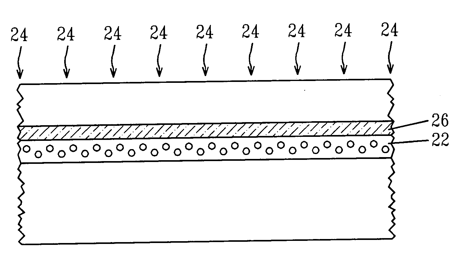
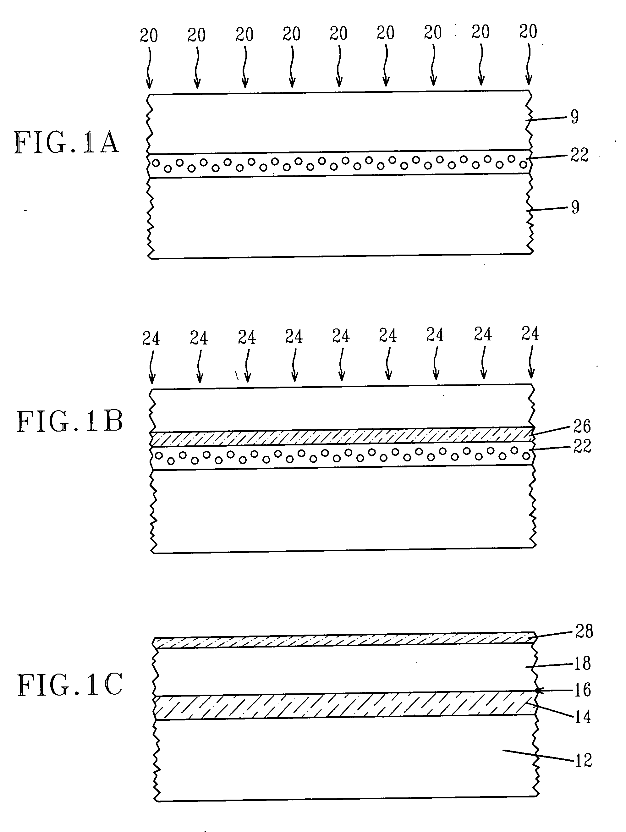
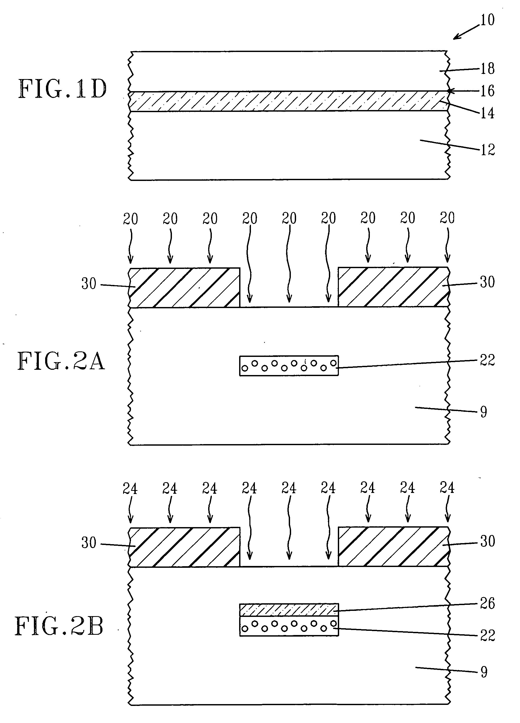
[0010] The present invention is aimed at improving the electrical quality of the entire BOX in SIMOX to that which is comparable to a thermal oxide. As stated above, the BOX of a SIMOX wafer essentially consists of two regions (i) a top region that is as good as a thermal oxide since it is formed by ITOX, and (ii) a bottom region where most of the implanted oxygen forms the oxide. The latter region contains non-stoichiometric SiO2 which has inferior electrical quality as compared to the top region.
[0012] In a highly preferred embodiment of the present invention, Steps (II) and (III) are implemented. In yet another embodiment of the present invention, Step (III) is implemented. In still yet another highly preferred embodiment of the present invention, all three of the aforementioned processing steps, i.e., Steps (I), (II) and (III), are implemented. It is emphasized that when a SIMOX process using step (III) of the present invention, the electrical quality of the BOX region is substantially improved, especially in the lower region of the BOX, since the soak cycle, i.e., pre-annealing step, prior to the ITOX anneal allows dissolution of Si and SiOx precipitates in the oxygen implanted region.
[0014] While some traditional SIMOX processes perform all the implant steps at the same energy, the present invention as described above in Steps (I) and (II) uses energies that are differentiated from one another, leading to new properties for the BOX. The exact combination of dose and energy and the offset between the two implants is key in producing improved BOX SIMOX. The improvement in the quality in the middle of the box region makes it particularly suited for process damaging environments.

Problems solved by technology

Although others may have produced BOX layers with good dielectric properties, the methods to produce BOX layers in SIMOX with extremely high dielectric properties after processing induced damage has not been documented.
As SOI complementary metal oxide semiconductor (CMOS) layers get thinner and the BOX layer becomes closer to the top surface of the substrate, it becomes vulnerable to certain processes, such as, for example, shallow trench formation, during which thinning of the top portion of the BOX can occur.
The BOX thinning makes it susceptible to breakdown.
Furthermore, certain plasma processes are known to cause BOX breakdown via charging through the BOX in the areas where BOX damage has originally occurred.
The primary one being that a thick BOX requires a much higher dose of oxygen implant, leading to a much longer and much more costly process.
Typically, the electrical quality of the BOX in commercial SIMOX is inferior to that of a thermal oxide.
The foregoing is why SIMOX wafers often show significant BOX degradation after process damage during the device fabrication (for example, BOX erosion by STI polishing or process charging).

Method used


Image

  • High electrical quality buried oxide in simox
  • High electrical quality buried oxide in simox
  • High electrical quality buried oxide in simox

Examples


example

[0059] An SOI wafer having a nominal Si thickness of about 700 Å and a high voltage BOX thickness of about 1450 Å was produced using the following processing steps: [0060] Starting bulk (100) Si substrate; [0061] Base dose oxygen implant: dose 2.1E17, energy 170 keV, wafer temperature 365° C.; [0062] Room temperature implant: dose 2.5E15, energy 158 keV, wafer temperature 25° C.; [0063] Pre-anneal 1300° C., 2 hours, argon ambient with less than 5% oxygen; [0064] ITOX anneal: 1300°-1320° C., 8 hours, argon ambient with about 50% oxygen; [0065] anneal: 1320° C., 5 hours, argon ambient with less than 5% oxygen; and [0066] strip surface oxide layer.

[0067] The above processing steps, which are representative of the present invention, achieved a BOX with increased breakdown through the entire BOX thickness. A graph of the BOX breakdown of the improved SIMOX process of the present invention is shown in FIG. 6. In FIG. 6, Curve X denotes the process of the present invention. In addition to...


PUM


Abstract

A SIMOX (separation by implanted oxygen) process is provided that forms a silicon-on-insulator (SOI) substrate having a buried oxide with improved electrical properties. The process implements at least one of the following processing steps into SIMOX: (I) lowering of the oxygen ion dose in the base oxygen ion implant step; (II) off-setting the implant energy of the room temperature (RT) implant step to a value that is about 5 to about 20% lower than the base ion implant step; and (III) creating a soak cycle, i.e., pre-annealing step, prior to the internal oxidation anneal which allows dissolution of Si and SiOx precipitates in the oxygen implanted region. The temperature and time of the soak cycle as well as the base implant dose are critical in determining the final BOX quality.

Description

FIELD OF THE INVENTION [0001] The present invention relates to silicon-on-insulator (SOI) substrates for use in the semiconductor industry, and more particularly to methods of forming SOI substrates wherein the buried oxide region has specific high breakdown properties when subjected to process damage and high-degree of process-induced charging. BACKGROUND OF THE INVENTION [0002] Separation by implanted oxygen (SIMOX) is one technique that is typically employed in fabricating SOI substrates that can be used in the manufacturing of integrated circuits (ICs). SIMOX typically involves using high-energy ions to implant oxygen ions beneath the surface of a bulk silicon substrate. During a subsequent high temperature annealing step which follows the implantation of oxygen ions, the implanted oxygen forms a layer of buried oxide (BOX) which electrically isolates a top silicon layer (i.e., the SOI layer) of the substrate from a bottom silicon layer. [0003] The implantation and annealing con...

Claims


Application Information

Patent Timeline
IPC IPC(8): H01L21/00H01L21/762H01L21/84
CPCH01L21/84H01L21/76243
Inventor DESOUZA, JOEL P.FOGEL, KEITH E.HOVEL, HAROLD J.LEE, JUNEDONGMAURER, SIEGFRIED L.SADANA, DEVENDRA K.SCHEPIS, DOMINIC J.
Owner GLOBALFOUNDRIES INC
Learn More