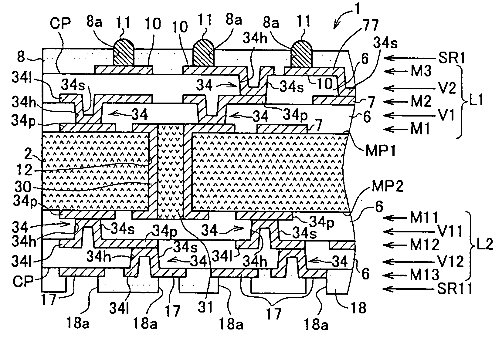
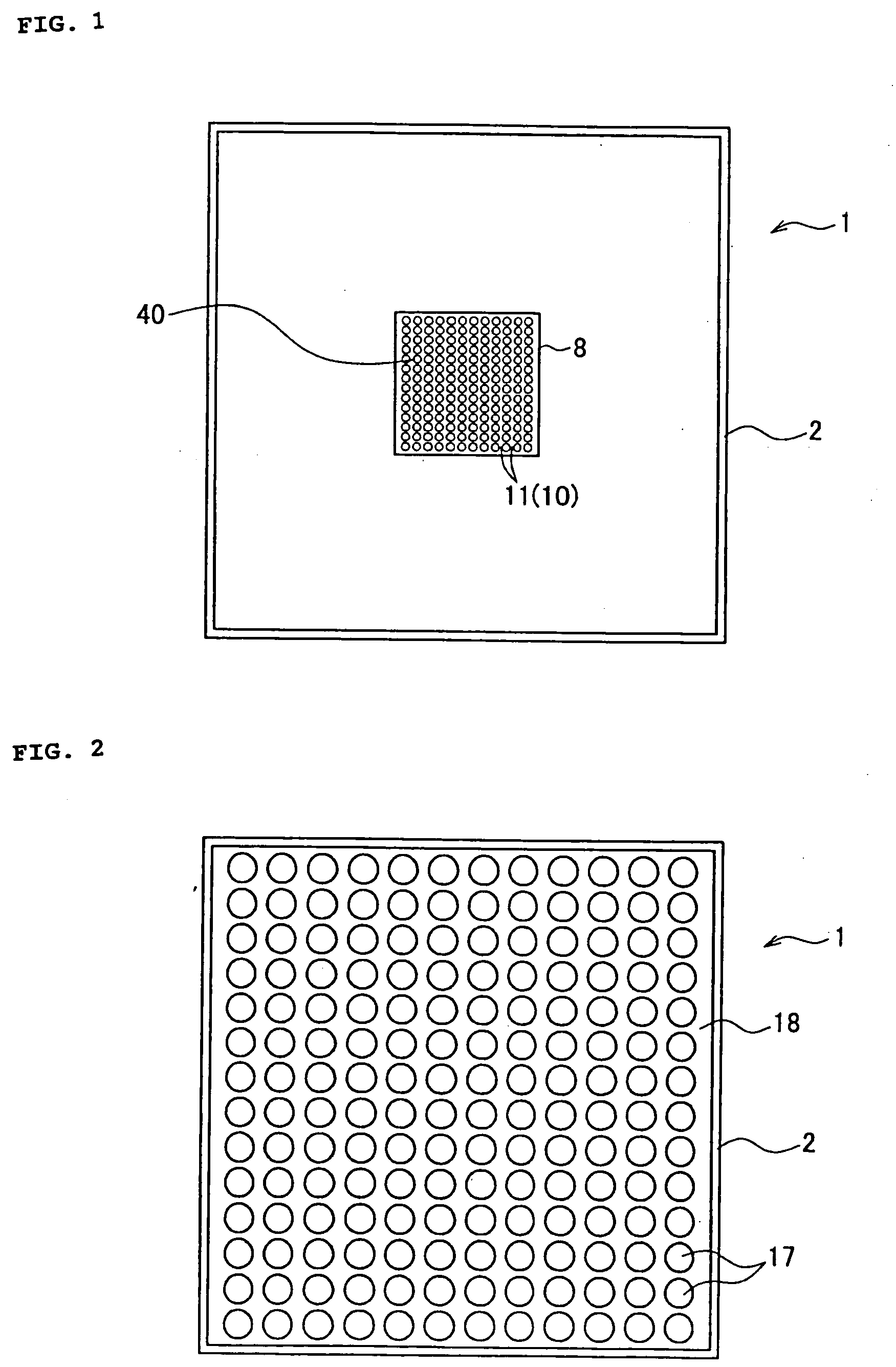
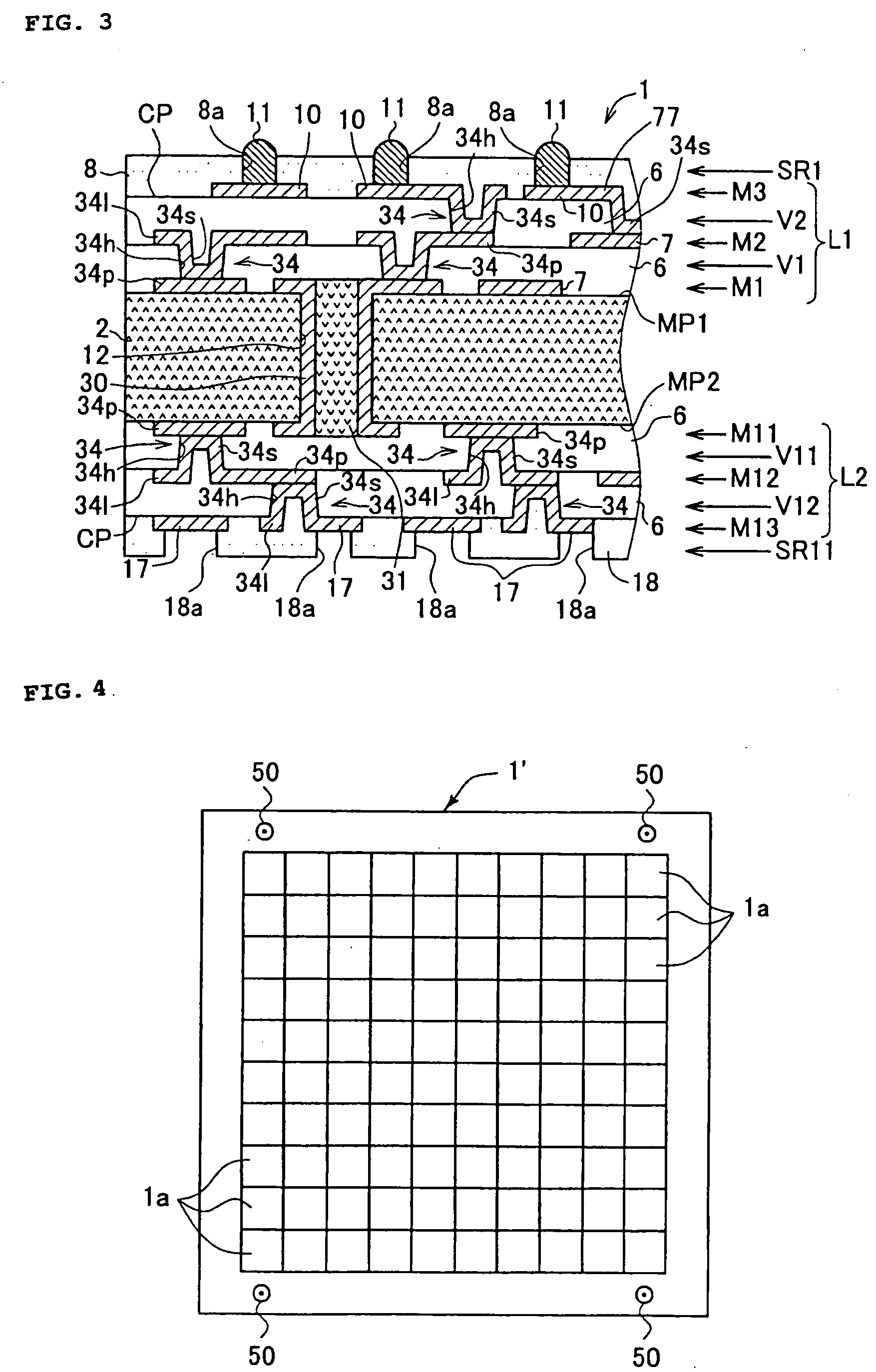
[0010] According to this embodiment of the present invention, by “reading out” or detecting the positioning mark formed on the wiring substrate workpiece by detecting reflected light, the position of the wiring substrate workpiece can be identified. The positioning mark, which, as noted above, is formed by removing an annular or ring-like portion of the resin
dielectric layer, is formed by irradiating laser during incremental shifting of the position of the
irradiation. Although any inaccuracy associated with the laser device will affect the accuracy of each
irradiation position, the
resultant disparity will be basically averaged out over the entire
irradiation positioning process. Further, because the laser irradiation is controlled so as to provide overlapping in a circumferential direction and a radial direction of the annular excavation area, smooth angular opening ends (i.e., the edges defining the annular groove of the positioning mark) can be formed on both the inside and outside opening ends of the positioning mark. For this reason, an improvement is provided in the detection accuracy in detecting the positioning mark with reflected light so that the identification accuracy of the position of the wiring substrate workpiece also is improved. Consequently, the method of this embodiment of the present invention enables further
miniaturization of the wiring pattern of the wiring substrate as compared with conventional methods.
[0012] In a preferred embodiment, in the step of forming the positioning mark, inner and outer circumferential reference lines are determined in the selected excavation area, laser irradiation positions are set up at predetermined angular intervals on each of the reference lines and the laser irradiation is successively projected onto the set irradiation positions. The ring-like shape of the groove varies depending on the size and
groove width. If the laser beam is controlled based on the reference lines, a balance can be achieved between high processing efficiency and success in obtaining a sharp contour opening edge.
[0014] Advantageously, in the step of forming the positioning mark, the dry film
resist is prevented from entering into the groove so as to maintain a uniform groove contour. In a preferred implementation, in the step for identifying the position of the wiring substrate workpiece, a camera for detecting reflected light is focused on the main surface of the resin dielectric layer so as to recognize opening ends of the groove of the positioning mark beneath the dry film
resist. The dry film
resist, used as a plating resist, is preferably prevented from entering into the groove by stretching the dry resist so as to avoid deflection thereof. Consequently, the recognition accuracy in recognizing the opening end of the groove constituting the positioning mark using reflected light is increased. Because this recognition accuracy is increased, the accuracy with which the position of the wiring substrate workpiece is identified is also improved. Moreover, although the positioning mark may be photographed through the dry resist film, the dry film resist is preferably disposed so as not to cover the positioning mark so that the positioning mark can be photographed directly.
[0015] In one embodiment, the resist is a liquid type resist which is applied directly to a wiring substrate workpiece, as well as a dry resist film having autonomy. When a liquid type resist is applied to the entire surface of the wiring substrate work, the situation is different from the case of the dry film resist because the liquid type resist will enter the groove constituting the positioning mark so that the groove is uniformly filled with the liquid type resist. If the dry film resist enters into the groove in a random or nonuniform manner, the reflection of the impinging light will be disturbed, and, as a consequence, the recognition accuracy, i.e., the accuracy with which the positioning mark is recognized, decreases. In contrast, because the liquid type resist uniformly fills the groove the reflection of the light is only minimally disturbed. Thus, the recognition accuracy of the positioning mark is excellent. However, because it is desirable that even the liquid type resist not enter into the groove if possible, it is preferable to apply the liquid type resist to the wiring substrate workpiece in such a way that the positioning mark is avoided, similarly to the case of the dry film resist.
[0016] According to another aspect of the present invention, in order to solve the basic above-described problem, there is provided a method for manufacturing a wiring substrate including a wiring integrated portion in which a resin dielectric layer and a conductor layer are alternately laminated, the manufacturing method comprising steps of: laminating the conductor layer and the resin dielectric layer on a supporting substrate with the dielectric layer outermost; forming a positioning mark by removing a portion of the resin dielectric layer to form a groove; and irradiating the positioning mark with position detecting light projected onto the main surface of the resin dielectric layer so that light is reflected therefrom; and detecting reflected light and identifying the position of a wiring substrate workpiece based on the reflected light detected, wherein, in the step of identifying the position of the wiring substrate workpiece, a camera for detecting the reflected light is focused on the main surface of the resin dielectric layer so as to recognize ends defining the groove of the positioning mark. According to this aspect of the present invention, the recognition property of the positioning mark is improved so that the identification accuracy of the position of the wiring substrate workpiece is also improved.

